Transcription of 4 MHz, 7 nV/√Hz, Low Offset and Drift, High Precision ...
1 4 MHz, 7 nV/ Hz, Low Offset and Drift, high Precision AmplifiersData Sheet ADA4077-1/ADA4077-2/ADA4077-4 Rev. E Document Feedback Information furnished by Analog Devices is believed to be accurate and reliable. However, no responsibility is assumed by Analog Devices for its use, nor for any infringements of patents or other rights of third parties that may result from its use. Specifications subject to change without notice. No license is granted by implication or otherwise under any patent or patent rights of Analog Devices. Trademarks and registered trademarks are the property of their respective owners.
2 One Technology Way, Box 9106, Norwood, MA 02062-9106, : 2012 2017 Analog Devices, Inc. All rights reserved. Technical Support FEATURES Offset voltage: 25 V maximum at 25 C (B grade, 8-lead SOIC, single/ dual) 50 V maximum at 25 C (A grade, 8-lead SOIC, single/ dual) 50 V maximum at 25 C (A grade, 14-lead SOIC, quad) Offset voltage drift: V/ C maximum (B grade, 8-lead SOIC, single/dual) V/ C maximum (A grade, 8-lead SOIC, single/dual) V/ C maximum (A grade, 14-lead SOIC, quad) MSL1 rated Low input bias current: 1 nA maximum at TA = 25 C Low voltage noise density: nV/ Hz typical at f = 1000 Hz CMRR, PSRR, and AV > 120 dB minimum Low supply current.
3 400 A per amplifier typical Wide gain bandwidth product: MHz at 5 V Dual-supply operation: Specified at 5 V to 15 V Operates at V to 15 V Unity gain stable No phase reversal Long-term Offset voltage drift (10,000 hours): V typical Temperature hysteresis: 1 V typical APPLICATIONS Process control front-end amplifiers Optical network control circuits Instrumentation Precision sensors and controls Precision filters GENERAL DESCRIPTION The single ADA4077-1, dual ADA4077-2, and quad ADA4077-4 amplifiers feature extremely low Offset voltage and drift, and low input bias current, noise, and power consumption.
4 Outputs are stable with capacitive loads of more than 1000 pF with no external compensation. Applications for this amplifier include sensor signal conditioning (such as thermocouples, resistance temperature detectors (RTDs), strain gages), process control front-end amplifiers, and Precision diode power measurement in optical and wireless transmission systems. The ADA4077-1/ADA4077-2/ADA4077-4 are useful in line powered and portable instrumentation, Precision filters, and voltage or current measurement and level setting. Unlike other amplifiers, the ADA4077-1/ADA4077-2/ ADA4077-4 have an MSL1 rating that is compliant with the most stringent of assembly processes, and they are specified over the extended industrial temperature range from 40 C to +125 C for the most demanding operating environments.
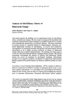
5 PIN CONNECTION DIAGRAMS NIC1 IN2+IN3V 4 NIC8V+7 OUT6 NIC5 NIC = NOT INTERNALLY VIEW(Not to Scale)10238-101 Figure 1. ADA4077-1, 8-Lead SOIC and 8-Lead MSOP OUT A1 IN A2+IN A3V 4V+8 OUT B7 IN B6+IN B5 ADA4077-2 TOP VIEW(Not to Scale)10238-001 Figure 2. ADA4077-2, 8-Lead MSOP and 8-Lead SOIC ADA4077-41234567 IN A+IN AV+OUT B IN B+IN BOUT A141312111098 IN D+IN DV OUT C IN C+IN COUT DTOP VIEW(Not to Scale)10238-202 Figure 3. ADA4077-4, 14-Lead TSSOP and 14-Lead SOIC The ADA4077-1 and ADA4077-2 are available in an 8-lead SOIC package, including the B grade, and in an 8-lead MSOP (A grade only). The ADA4077-4 is offered in a 14-lead TSSOP and a 14-lead SOIC package.
6 VOS ( V) 50 45 40 35 30 25 20 15 10 505 NUMBER OF AMPLIFIERS101520253035404550 MORE02040608010012014016018020010238-103 VSY = 5 VSOIC Figure 4. Offset Voltage Distribution Table 1. Evolution of Precision Devices by Generation Op Amp First Second Third Fourth Fifth Sixth Single OP07 OP77 OP177 OP1177 AD8677 ADA4077-1 Dual OP2177 ADA4077-2 Quad OP4177 ADA4077-4 ADA4077-1/ADA4077-2/ADA4077-4 Data SheetRev. E | Page 2 of 27 TABLE OF CONTENTS Features.
7 1 Applications .. 1 General Description .. 1 Pin Connection Diagrams .. 1 Revision History .. 2 Specifications .. 3 Electrical Characteristics, 5 V .. 3 Electrical Characteristics, 15 V .. 5 Absolute Maximum Ratings .. 7 Thermal Resistance .. 7 ESD Caution .. 7 Pin Configurations and Function Descriptions .. 8 Typical Performance Characteristics .. 11 Test Circuit .. 21 Theory of Operation .. 22 Applications Information .. 23 Output Phase Reversal .. 23 Low Power Linearized RTD .. 23 Proper Board Layout .. 23 Long-Term Drift .. 24 Temperature Hysteresis .. 24 Outline Dimensions .. 25 Ordering Guide .. 27 REVISION HISTORY 5/2017 Rev.
8 D to Rev. E Changes to Features Section, Applications Section, and Figure 1 .. 1 Added Maximum Reflow Temperature (MSL1 Rating) Parameter and Note 2,Table 4; Renumbered Sequentially .. 7 Changes to Figure 5, Figure 6, and Table 6 .. 8 Changes to Figure 24 and Figure 27 .. 13 Changes to Figure 29, Figure 30, Figure 31, Figure 32, Figure 33, and Figure 34 .. 14 Changes to Figure 66 .. 20 Added Test Circuit Section and Figure 69; Renumbered Sequentially .. 22 Added Long-Term Drift Section, Temperature Hysteresis Section, Figure 72, Figure 73, and Figure 74 .. 24 Changes to Ordering Guide .. 27 10/2016 Rev. C to Rev.
9 D Changes to Table 2 .. 3 Changes to Table 3 .. 5 Changes to Figure 19 .. 12 Changes to Figure 23 and Figure 26 .. 13 Changes to Figure 29, Figure 30, Figure 32, and Figure 33 .. 14 6/2015 Rev. B to Rev. C Change to Figure 63 .. 18 1/2014 Rev. A to Rev. B Added ADA4077-1 .. Universal Changes to Features Section .. 1 Added Figure 1; Renumbered Sequentially .. 1 Changes to Table 2 .. 3 Changes to Table 3 .. 4 Added Figure 5, Figure 6, and Table 6; Renumbered Sequentially .. 7 Changes to Figure 17, Figure 20, and Figure 21 .. 11 Changes to Figure 65 .. 19 Added Figure 67 and Figure 68 .. 19 Changes to Output Phase Reversal Section and Figure 70.
10 21 Changes to Ordering Guide .. 24 10/2013 Rev. 0 to Rev. A Added ADA4077-4 .. Universal Changes to Features, General Description, and Figure 1 .. 1 Deleted Figure 2; Renumbered Sequentially .. 1 Added Figure 2 .. 1 Changes to Table 2 .. 3 Changes to Table 3 .. 4 Changes to Table 4 .. 6 Added Figure 6, Figure 7, and Table 7; Renumbered Sequentially .. 8 Changes to Typical Performance Characteristics Section .. 9 Changes to Figure 65 .. 20 Updated Outline Dimensions .. 21 Changes to Ordering Guide .. 23 10/2012 Revision 0: Initial Version Data Sheet ADA4077-1/ADA4077-2/ADA4077-4 Rev. E | Page 3 of 27 SPECIFICATIONS ELECTRICAL CHARACTERISTICS, 5 V VSY = V, VCM = 0 V, TA = 25 C, unless otherwise noted.