Transcription of 5 kV rms Signal and Power Isolated RS-485 …
1 5 kV rms Signal and Power Isolated RS-485 transceiver with 15 kV ESD protection data sheet adm2682e / adm2687e Rev. C Document Feedback Information furnished by analog devices is believed to be accurate and reliable. However, no responsibility is assumed by analog devices for its use, nor for any infringements of patents or other rights of third parties that may result from its use. Specifications subject to change without notice. No license is granted by implication or otherwise under any patent or patent rights of analog devices . Trademarks and registered trademarks are the property of their respective owners. One Technology Way, Box 9106, Norwood, MA 02062-9106, Tel: 2011 2015 analog devices , Inc. All rights reserved. Technical Support FEATURES 5 kV rms Isolated RS-485 /RS-422 transceiver , configurable as half or full duplex isoPower integrated Isolated dc-to-dc converter 15 kV ESD protection on RS-485 input/output pins Complies with ANSI/TIA/EIA-485-A-98 and ISO 8482:1987(E) data rate: 16 Mbps ( adm2682e ), 500 kbps ( adm2687e ) 5 V or V operation Connect up to 256 nodes on one bus Open- and short-circuit, fail-safe receiver inputs High common-mode transient immunity: >25 kV/ s Thermal shutdown protection Safety and regulatory approvals UL recognition 5000 V rms for 1 minute per UL 1577 CSA Component Acceptance Notice #5A (pending) IEC 60601-1: 400 V rms (basic), 250 V rms (reinforced) IEC 60950-1: 600 V rms (basic), 380 V rms (reinforced) VDE Certificates of Conformity DIN V VDE V 0884-10 (VDE V 0884-10).
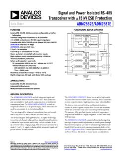
2 2006-12 VIORM = 846 V peak Operating temperature range: 40 C to +85 C 16-lead wide-body SOIC with >8 mm creepage and clearance APPLICATIONS Isolated RS-485 /RS-422 interfaces Industrial field networks Multipoint data transmission systems FUNCTIONAL BLOCK DIAGRAM 09927-001 adm2682e /ADM2687 ETxDABYZDEVCCVCCRxDREGND1 GND2 DECODEDRDECODEENCODEOSCILLATORRECTIFIERR EGULATORVISOOUTisoPower DC-TO-DCCONVERTERVISOINDIGITAL ISOLATIONiCouplerENCODEENCODEDECODETRANS CEIVERISOLATIONBARRIER Figure 1. GENERAL DESCRIPTION The adm2682e / adm2687e are fully integrated 5 kV rms Signal and Power Isolated data transceivers with 15 kV ESD protection and are suitable for high speed communication on multipoint transmission lines. The adm2682e / adm2687e include an integrated 5 kV rms Isolated dc-to-dc Power supply that eliminates the need for an external dc-to-dc isolation block.
3 They are designed for balanced transmission lines and comply with ANSI/TIA/EIA-485-A-98 and ISO 8482:1987(E). The devices integrate analog devices , Inc., iCoupler technology to combine a 3-channel isolator, a three-state differential line driver, a differential input receiver, and analog devices isoPower dc-to-dc converter into a single package. The devices are powered by a single 5 V or V supply, realizing a fully integrated Signal and Power Isolated RS-485 solution. The adm2682e / adm2687e drivers have an active high enable. An active low receiver enable is also provided, which causes the receiver output to enter a high impedance state when disabled. The devices have current limiting and thermal shutdown features to protect against output short circuits and situations where bus contention may cause excessive Power dissipation.
4 The parts are fully specified over the industrial temperature range and are available in a highly integrated, 16-lead, wide-body SOIC package with >8 mm creepage and clearance. The adm2682e / adm2687e contain isoPower technology that uses high frequency switching elements to transfer Power through the transformer. Special care must be taken during printed circuit board (PCB) layout to meet emissions standards. Refer to AN-0971 Application Note, Recommendations for Control of Radiated Emissions with isoPower devices , for details on board layout considerations. adm2682e / adm2687e data sheet Rev. C | Page 2 of 24 TABLE OF CONTENTS Features .. 1 Applications .. 1 Functional Block Diagram .. 1 General Description .. 1 Revision History .. 2 Specifications .. 3 adm2682e Timing Specifications .. 4 adm2687e Timing Specifications.
5 4 Package Characteristics .. 4 Regulatory Information .. 5 Insulation and Safety-Related Specifications .. 5 VDE 0884-10 Insulation Characteristics .. 6 Absolute Maximum Ratings .. 7 ESD Caution .. 7 Pin Configuration and Function Descriptions .. 8 Typical Performance Characteristics .. 9 Test Circuits .. 14 Switching Characteristics .. 15 Circuit 16 Signal Isolation .. 16 Power Isolation .. 16 Tr u t h Ta b l e 16 Thermal Shutdown .. 16 Open- and Short-Circuit, Fail-Safe Receiver 16 DC Correctness and Magnetic Field 16 Applications Information .. 18 PCB Layout .. 18 EMI Considerations .. 18 Insulation Lifetime .. 19 Isolated Supply Considerations .. 19 Typical Applications .. 20 Outline Dimensions .. 22 Ordering Guide .. 22 REVISION HISTORY 6/15 Rev. B to Rev. C Changes to Figure 1.
6 1 11/13 Rev. A to Rev. B Change to Features Section .. 1 Change to Table 5 .. 5 Changes to VDE 0884-10 Insulation Characteristics Section .. 6 6/13 Rev. 0 to Rev. A Updated UL and VDE Certification (Throughout) .. 1 Updated Outline Dimensions .. 22 Changes to Ordering Guide .. 22 7/11 Revision 0: Initial Version data sheet adm2682e / adm2687e Rev. C | Page 3 of 24 SPECIFICATIONS All voltages are relative to their respective ground; VCC V. All minimum/maximum specifications apply over the entire recommended operation range, unless otherwise noted. All typical specifications are at TA = 25 C, VCC = 5 V unless otherwise noted. Table 1. Parameter Symbol Min Typ Max Unit Test Conditions/Comments adm2687e SUPPLY CURRENT ICC data Rate 500 kbps 90 mA VCC = V, 100 load between Y and Z 72 mA VCC = 5 V, 100 load between Y and Z 125 mA VCC = V, 54 load between Y and Z 98 mA VCC = 5 V, 54 load between Y and Z 140 mA 120 load between Y and Z adm2682e SUPPLY CURRENT ICC data Rate = 16 Mbps 175 mA 120 load between Y and Z 260 mA 54 load between Y and Z data Rate = 16 Mbps, VCC V 130 mA 120 load between Y and Z 200 mA 54 load between Y and Z Isolated SUPPLY VOLTAGE VISOOUT V DRIVER Differential Outputs Differential Output Voltage, Loaded |VOD2| V RL = 100 (RS-422), see Figure 29 V RL = 54 ( RS-485 )
7 , see Figure 29 |VOD3| V 7 V VTEST1 12 V, see Figure 30 |VOD| for Complementary Output States |VOD| V RL = 54 or 100 , see Figure 29 Common-Mode Output Voltage VOC V RL = 54 or 100 , see Figure 29 |VOC| for Complementary Output States |VOC| V RL = 54 or 100 , see Figure 29 Short-Circuit Output Current IOS 200 mA Output Leakage Current (Y, Z) IO 30 A DE = 0 V, RE = 0 V, VCC = 0 V or V, VIN = 12 V 30 A DE = 0 V, RE = 0 V, VCC = 0 V or V, VIN = 7 V Logic Inputs DE, RE, TxD Input Threshold Low VIL VCC V DE, RE, TxD Input Threshold High VIH VCC V DE, RE, TxD Input Current II 10 10 A DE, RE, TxD RECEIVER Differential Inputs Differential Input Threshold Voltage VTH 200 125 30 mV 7 V < VCM < +12 V Input Voltage Hysteresis VHYS 15 mV VOC = 0 V Input Current (A, B)
8 II 125 A DE = 0 V, VCC = 0 V or V, VIN = 12 V 100 A DE = 0 V, VCC = 0 V or V, VIN = 7 V Line Input Resistance RIN 96 k 7 V < VCM < +12 V Logic Outputs Output Voltage Low VOL V IO = mA, VA VB = V Output Voltage High VOH VCC VCC V IO = mA, VA VB = V Short-Circuit Current 100 mA COMMON-MODE TRANSIENT IMMUNITY1 25 kV/ s VCM = 1 kV, transient magnitude = 800 V 1 CM is the maximum common-mode voltage slew rate that can be sustained while maintaining specification-compliant operation. VCM is the common-mode potential difference between the logic and bus sides. The transient magnitude is the range over which the common-mode is slewed. The common-mode voltage slew rates apply to both rising and falling common-mode voltage edges. adm2682e / adm2687e data sheet Rev.
9 C | Page 4 of 24 adm2682e TIMING SPECIFICATIONS TA = 40 C to +85 C. Table 2. Parameter Symbol Min Typ Max Unit Test Conditions/Comments DRIVER
10 Maximum data Rate 16 Mbps Propagation Delay, Low to High tDPLH 63 100 ns RL = 54 , CL1 = CL2 = 100 pF, see Figure 31 and Figure 35 Propagation Delay, High to Low tDPHL 64 100 ns RL = 54 , CL1 = CL2 = 100 pF, see Figure 31 and Figure 35 Output Skew tSKEW 1 8 ns RL = 54 , CL1 = CL2 = 100 pF, see Figure 31 and Figure 35 Rise Time/Fall Time tDR, tDF 15 ns RL = 54 , CL1 = CL2 = 100 pF, see Figure 31 and Figure 35 Enable Time tZL, tZH 120 ns RL = 110 , CL = 50 pF, see Figure 32 and Figure 37 Disable Time tLZ, tHZ 150 ns RL = 110 , CL = 50 pF, see Figure 32 and Figure 37 RECEIVER Propagation Delay, Low to High tRPLH 94 110 ns CL = 15 pF.