Transcription of 50 mA/500 mA, High Efficiency, Ultralow Power …
1 50 mA/500 mA, high efficiency , Ultralow Power step - down Regulator Data Sheet ADP5301. FEATURES TYPICAL APPLICATION CIRCUIT. Input start-up voltage range: V to V. VIN = H VOUT. Operates down to V voltage PVIN SW. Ultralow 180 nA quiescent current with no load 10 F. ADP5301 10 F. Selectable output voltage of V to V or V to V (9-BALL WLCSP). ON. output accuracy over full temperature range in OFF. EN PGND. PWM mode PWM. 13169-001. Selectable hysteresis mode or PWM operation mode HYS. SYNC/ FB. MODE. Output current VID0: VID8: Up to 50 mA in hysteresis mode VOUTOK VID VID1: VID9: Up to 500 mA in PWM mode RVID. VID2: VID3: VID10: VID11: VOUTOK flag monitors the output voltage AGND. VID4: VID5: VID12: VID13: 100% duty cycle operation mode VID6: VID7: VID14: VID15: 2 MHz switching frequency with optional synchronization Figure 1.
2 Input from MHz to MHz QOD option UVLO, OCP, and TSD protection 9-ball, mm mm WLCSP. 40 C to +125 C junction temperature APPLICATIONS. Energy (gas and water) metering Portable and battery-powered equipment Medical applications Keep-alive Power supplies GENERAL DESCRIPTION. The ADP5301 is a high efficiency , Ultralow quiescent current The ADP5301 contains a VOUTOK flag, which monitors the step - down regulator that draws only a 180 nA quiescent current output voltage and runs at a 2 MHz switching frequency in to regulate the output at no load. PWM mode. SYNC/MODE can synchronize to an external The ADP5301 runs from an input startup voltage range of V clock from MHz to MHz. to V, allowing the use of multiple alkaline/NiMH, Li-Ion Other key features in the ADP5301 include separate enabling, cells, or other Power sources. The output voltage is selectable from quick output discharge (QOD), and safety features such as V to V by an external VID resistor and factory fuse.
3 The overcurrent protection (OCP), thermal shutdown (TSD), and total solution requires only four tiny external components. input undervoltage lockout (UVLO). The ADP5301 can operate between hysteresis mode and PWM The ADP5301 is available in a 9-ball, mm mm mode via the SYNC/MODE pin. The regulator in hysteresis mode WLCSP rated for a 40 C to +125 C junction temperature range. achieves excellent efficiency at a Power of less than 1 mW and provides up to 50 mA of output current. The regulator in PWM. mode produces a lower output ripple and supplies up to 500 mA. of output current. The flexible configuration capability during operation of the device enables very efficient Power management to meet both the longest battery life and low system noise requirements. Rev. B Document Feedback Information furnished by analog devices is believed to be accurate and reliable.
4 However, no responsibility isassumed by analog Devicesfor its use,norfor any infringements of patents or other rights of third parties thatmay resultfrom its to One Technology Way, Box 9106, Norwood, MA 02062-9106, license is granted by implication or otherwise under any patent or patent rights of analog devices . Tel: 2015 2016 analog devices , Inc. All rights reserved. Trademarks and registered trademarks are the property of their respective owners. Technical Support ADP5301 Data Sheet TABLE OF CONTENTS. 1 Short-Circuit Protection .. 15. Applications .. 1 Soft 15. Typical Application 1 Startup with a Precharged 15. General Description .. 1 100% Duty Cycle Operation .. 15. Revision History .. 2 Active Discharge .. 15. Functional Block 3 VOUTOK 15. Specifications .. 4 Thermal 15. Absolute Maximum Ratings .. 6 Applications 16.
5 Thermal Resistance .. 6 External Component 16. ESD 6 Selecting the Inductor .. 16. Pin Configuration and Function 7 Output 16. Typical Performance 8 Input 17. Theory of 14 17. Buck Regulator Operation 14 Printed Circuit Board (PCB) Layout Recommendations .. 18. Oscillator and Synchronization .. 14 Typical Application Circuits .. 19. Adjustable and Fixed Output 14 Factory Programmable 20. Undervoltage Lockout (UVLO).. 15 Outline Dimensions .. 21. Enable/Disable .. 15 Ordering 21. Current 15. REVISION HISTORY. 6/2016 Rev. A to Rev. B 12/2015 Rev. 0 to Rev. A. Changes to Features Section and General Description Section ..1 Changes to Ordering Guide ..21. Change to SYNC Clock Range Parameter, Table Change to Table 4 ..7 6/2015 Revision 0: Initial Version Change to Oscillator and Synchronization Section ..14. Changes to Table Rev.
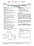
6 B | Page 2 of 21. Data Sheet ADP5301. FUNCTIONAL BLOCK DIAGRAM. PVIN. PVIN. VOUTOK 90%. 87% DRIVER. ILIM_PWM. FB. SW. ILIM_HYS. CONTROL (PWM). LOGIC 0A(HYS). PWM PVIN. SLOPE . DRIVER. COMPENSATION PGND. STANDBY. FB. INTERNAL. FEEDBACK. RESISTOR. VID. DIVIDER. V TO I. MODE. SOFT. AGND. START. EN BAND GAP BIAS. AND. PVIN HOUSEKEEPING. UVLO. SYNC 2 MHz SYNC/ OSC. MODE MODE. KEEP ALIVE BLOCK. 13169-002. Figure 2. Rev. B | Page 3 of 21. ADP5301 Data Sheet SPECIFICATIONS. VIN = V, VOUT = V, TJ = 40 C to +125 C for minimum and maximum specifications, and TA = 25 C for typical specifications, unless otherwise noted. Table 1. Parameter Symbol Min Typ Max Unit Test Conditions/Comments INPUT SUPPLY VOLTAGE RANGE VIN V. SHUTDOWN CURRENT ISHUTDOWN 18 40 nA VEN = 0 V, 40 C TJ +85 C. 18 130 nA VEN = 0 V, 40 C TJ +125 C. QUIESCENT CURRENT.
7 Operating Quiescent Current in Hysteresis Mode IQ_HYS 180 260 nA 40 C TJ +85 C. 180 350 nA 40 C TJ +125 C. 570 1400 nA 100% duty cycle operation, VIN = V, VOUT set to V. Operating Quiescent Current in PWM Mode IQ_PWM 425 630 A. UNDERVOLTAGE LOCKOUT UVLO. UVLO Threshold Rising VUVLO_RISING V. Falling VUVLO_FALLING V. OSCILLATOR CIRCUIT. Switching Frequency in PWM Mode fSW MHz FB Threshold of Frequency Fold VOSC_FOLD V. SYNCHRONIZATION THRESHOLD. SYNC Clock Range SYNCCLOCK MHz SYNC high Level Threshold SYNCHIGH V. SYNC Low Level Threshold SYNCLOW V. SYNC Duty Cycle Range SYNCDUTY 100 1/fSW ns 150. SYNC/MODE Leakage Current ISYNC_LEAKAGE 50 150 nA VSYNC/MODE = V. MODE TRANSITION. Transition Delay from Hysteresis Mode to tHYS_TO_PWM 20 Clock SYNC/MODE goes logic high from PWM Mode cycles logic low EN PIN. Input Voltage Threshold high VIH V.
8 Low VIL V. Input Leakage Current IEN_LEAKAGE 25 nA. FB PIN. Output Options by VID Resistor VOUT_OPT V V to V in various factory options PWM Mode Fixed VID Code Voltage Accuracy VFB_PWM_FIX + % TJ = 25 C, output voltage setting via factory fuse + % 40 C TJ +125 C. Adjustable VID Code Voltage Accuracy VFB_PWM_ADJ + % Output voltage setting via VID resistor Hysteresis Mode Fixed VID Code Threshold Accuracy from VFB_HYS_FIX + % TJ = 25 C. Active Mode to Standby Mode + % 40 C TJ +125 C. Adjustable VID Code Threshold Accuracy VFB_HYS_ADJ 3 +3 % 40 C TJ +125 C. from Active Mode to Standby Mode Hysteresis of Threshold Accuracy from VFB_HYS (HYS) 1 %. Active Mode to Standby Mode Feedback Bias Current IFB 66 95 nA Output Option 0, VOUT = V. 25 45 nA Output Option 1, VOUT = V. Rev. B | Page 4 of 21. Data Sheet ADP5301. Parameter Symbol Min Typ Max Unit Test Conditions/Comments SW PIN.
9 high -Side Power FET On Resistance RDS (ON) H 324 470 m Pin to pin measurement Low-Side Power FET On Resistance RDS (ON) L 196 320 m Pin to pin measurement Current-Limit in PWM Mode ILIM_PWM 800 1000 1200 mA SYNC/MODE = high Peak Current in Hysteresis Mode ILIM_HYS 265 mA SYNC/MODE = low Minimum On Time tMIN_ON 40 70 ns VOUTOK PIN. Monitor Threshold VOUTOK (RISE) 87 90 93 %. Monitor Hysteresis VOUTOK (HYS) 3 %. Monitor Rising Delay tVOUTOK_RISE 40 s Monitor Falling Delay tVOUTOK_FALL 10 s Leakage Current IVOUTOK_LEAKAGE 1 A. Output Low Voltage VOUTOK_LOW 50 80 mV IVOUTOK = 100 A. SOFT START. Default Soft Start Time tSS 350 s Factory trim, 1 bit (350 s and 2800 s). Start-Up Delay tSTART_DELAY 2 ms Delay from the EN pin being pulled high COUT DISCHARGE SWITCH ON RESISTANCE RDIS 290 . THERMAL SHUTDOWN. Threshold TSHDN 142 C.
10 Hysteresis THYS 127 C. Rev. B | Page 5 of 21. ADP5301 Data Sheet ABSOLUTE MAXIMUM RATINGS. Table 2. THERMAL RESISTANCE. Parameter Rating JA is specified for the worst case conditions, that is, a device PVIN to PGND V to +7 V soldered in a circuit board for surface-mount packages. SW to PGND V to PVIN + V. Table 3. Thermal Resistance FB to AGND V to +7 V. VID to AGND V to +7 V Package Type JA Unit EN to AGND V to +7 V 9-Ball WLCSP 132 C/W. VOUTOK to AGND V to +7 V. SYNC/MODE to AGND V to +7 V ESD CAUTION. PGND to AGND V to + V. Storage Temperate Range 65 C to +150 C. Operational Junction Temperature Range 40 C to +125 C. Stresses at or above those listed under Absolute Maximum Ratings may cause permanent damage to the product. This is a stress rating only; functional operation of the product at these or any other conditions above those indicated in the operational section of this specification is not implied.