Transcription of 8/10/12-Bit Voltage Output Digital-to-Analog …
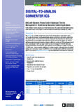
1 2010 Microchip Technology 1 MCP4901/4911/4921 Features MCP4901: 8-Bit Voltage Output DAC MCP4911: 10-Bit Voltage Output DAC MCP4921: 12-Bit Voltage Output DAC Rail-to-Rail Output SPI Interface with 20 MHz Clock Support Simultaneous Latching of the DAC Output with LDAC Pin Fast Settling Time of s Selectable Unity or 2x Gain Output External Voltage Reference Input External Multiplier Mode to Single-Supply Operation Extended Temperature Range: -40 C to +125 CApplications Set Point or Offset Trimming Precision Selectable Voltage Reference Motor Control Feedback Loop Digitally-Controlled Multiplier/Divider Calibration of Optical Communication DevicesRelated ProductsDescriptionThe MCP4901/4911/4921 devices are single channel8-bit, 10-bit and 12-bit buffered Voltage outputDigital-to- analog Converters (DACs), respectively. Thedevices operate from a single to supply withan SPI compatible Serial Peripheral Interface.
2 The usercan configure the full-scale range of the device to beVREF or 2*VREF by setting the gain selection option bit(gain of 1 of 2).The user can shut down the device by setting the Con-figuration Register bit. In Shutdown mode, most of theinternal circuits are turned off for power savings, andthe Output amplifier is configured to present a knownhigh resistance Output load (500 k typical . The devices include double-buffered registers,allowing synchronous updates of the DAC Output usingthe LDAC pin. These devices also incorporate aPower-on Reset (POR) circuit to ensure reliable devices utilize a resistive string architecture, withits inherent advantages of low Differential Non-Linear-ity (DNL) error and fast settling time. These devices arespecified over the extended temperature range(+125 C).The devices provide high accuracy and low noiseperformance for consumer and industrial applicationswhere calibration or compensation of signals (such astemperature, pressure and humidity) are required.)
3 The MCP4901/4911/4921 devices are available in thePDIP, SOIC, MSOP and DFN packages. Package TypesP/NDAC ResolutionNo. of ChannelsVoltage Reference(VREF)MCP480181 Internal( )MCP4811101 MCP4821121 MCP480282 MCP4812102 MCP4822122 MCP490181 ExternalMCP4911101 MCP4921121 MCP490282 MCP4912102 MCP4922122 Note: The products listed here have similar AC/DC performances. DFN-8 (2x3)*12348765 CSSCKSDIVDDVSSVOUTLDACMCP4901: 8-bit single DACMCP4911: 10-bit single DACMCP4921: 12-bit single DACMCP49x18-Pin PDIP, SOIC, MSOP12348765 CSSCKSDIVDDVSSVOUTLDACVREFVREFEP9* Includes Exposed Thermal Pad (EP); see Ta b l e 3 - Voltage Output Digital-to-Analog Converter with SPI InterfaceMCP4901/4911/4921DS22248A-page 2 2010 Microchip Technology DiagramOp AmpVDDVSSCSSDISCKI nterface LogicInput RegisterDAC RegisterStringDACP ower-on ResetVOUTLDACO utputGainLogicOutputLogicVREFB uffer 2010 Microchip Technology 3 MCP4901/4911 CHARACTERISTICSA bsolute Maximum Ratings inputs and outputs.
4 VSS to VDD+ Current at Input Pins .. 2 mACurrent at Supply Pins .. 50 mACurrent at Output Pins .. 25 mAStorage temperature ..-65 C to +150 CAmbient temp. with power applied ..-55 C to +125 CESD protection on all pins 4 kV (HBM), 400V (MM)Maximum Junction Temperature (TJ) ..+150 C Notice: Stresses above those listed under MaximumRatings may cause permanent damage to the device. This isa stress rating only and functional operation of the device atthose or any other conditions above those indicated in theoperational listings of this specification is not to maximum rating conditions for extended periodsmay affect device CHARACTERISTICSE lectrical Specifications: Unless otherwise indicated, VDD = 5V, VSS = 0V, VREF = , Output Buffer Gain (G) = 2x, RL = 5 k to GND, CL = 100 pF TA = -40 to +85 C. Typical values are at +25 RequirementsOperating CurrentIDD 175350 AVDD = 5 VVDD = 3 VVREF input is unbuffered, all digital inputs are grounded, all analog outputs (VOUT) are unloaded.
5 Code = 0x000h 125250 ASoftware Shutdown Current ISHDN_SW APower-on Reset circuit remains onPower-On-Reset ThresholdVPOR VDC AccuracyMCP4901 Resolutionn8 Bits INL ErrorINL-1 DNL + 1 MCP4911 Resolutionn10 Bits INL + 1 MCP4921 Resolutionn12 Bits INL ErrorINL-12 212 LSb + 1 Note 1:Guaranteed monotonic by design over all :This parameter is ensured by design, and not 100% 4 2010 Microchip Technology ErrorVOS of FSRCode = 0x000hOffset Error TemperatureCoefficientVOS/ C ppm/ C -45 C to 25 C ppm/ C +25 C to 85 CGain Error gE of FSRCode = 0xFFFh, not including offset errorGain Error Temperature Coefficient G/ C -3 ppm/ CInput Amplifier (VREF Input)Input Range Buffered VDD 2 Code = 2048 VREF = Vp-p, f = 100 Hz and 1kHzInput Range Unbuffered ModeVREF0 VDDVI nput ImpedanceRVREF 165 k Unbuffered ModeInput Capacitance Unbuffered ModeCVREF 7 pFMultiplier Mode -3 dB BandwidthfVREF 450 kHzVREF = , Unbuffered, G = 1fVREF 400 kHzVREF = Vp-p, Unbuffered, G = 2 Multiplier Mode Total Harmonic DistortionTHDVREF -73 dBVREF = ,Frequency = 1 kHzOutput AmplifierOutput SwingVOUT to VDD VAccuracy is better than 1 LSb for VOUT = 10 mV to (VDD 40 mV)
6 Phase Margin m 66 DegreesSlew RateSR V/ sShort Circuit CurrentISC 15 24 mASettling Timetsettling sWithin 1/2 LSB of final value from 1/4 to 3/4 full-scale rangeDynamic Performance (Note 2)DAC-to-DAC Crosstalk 10 nV-sMajor Code Transition Glitch 45 nV-s1 LSB change around major carry ( to ) digital Feedthrough 10 nV-sAnalog Crosstalk 10 nV-sELECTRICAL CHARACTERISTICS (CONTINUED)Electrical Specifications: Unless otherwise indicated, VDD = 5V, VSS = 0V, VREF = , Output Buffer Gain (G) = 2x, RL = 5 k to GND, CL = 100 pF TA = -40 to +85 C. Typical values are at +25 1:Guaranteed monotonic by design over all :This parameter is ensured by design, and not 100% tested. 2010 Microchip Technology 5 MCP4901/4911/4921 ELECTRICAL CHARACTERISTIC WITH EXTENDED TEMPERATUREE lectrical Specifications: Unless otherwise indicated, VDD = 5V, VSS = 0V, VREF = , Output Buffer Gain (G) = 2x, RL = 5 k to GND, CL = 100 pF.
7 Typical values are at +125 C by characterization or RequirementsInput CurrentIDD 200 AVREF input is unbuffered, all digi-tal inputs are grounded, all analog outputs (VOUT) are unloaded. Code = 0x000hSoftware Shutdown Current ISHDN_SW 5 APower-on Reset ThresholdVPOR VDC AccuracyMCP4901 Resolutionn8 Bits INL ErrorINL DNL DNL 1 MCP4911 Resolutionn10 Bits INL ErrorINL 1 LSb DNLDNL 1 MCP4921 Resolutionn12 Bits INL ErrorINL 4 LSb DNLDNL 1 Offset ErrorVOS % of FSRCode = 0x000hOffset Error TemperatureCoefficientVOS/ C -5 ppm/ C+25 C to +125 CGain Error gE % of FSRCode = 0xFFFh, not including offset errorGain Error Temperature Coefficient G/ C -3 ppm/ CInput Amplifier (VREF Input)Input Range Buffered ModeVREF to VNote 1 Code = 2048, VREF = Vp-p, f = 100 Hz and 1kHzInput Range Unbuffered ModeVREF0 VDDVI nput ImpedanceRVREF 174 k Unbuffered ModeInput Capacitance Unbuffered ModeCVREF 7 pFMultiplying Mode -3 dB BandwidthfVREF 450 kHzVREF = Vp-p, Unbuffered, G = 1xfVREF 400 kHzVREF = Vp-p, Unbuffered, G = 2xNote 1:Guaranteed monotonic by design over all.
8 This parameter is ensured by design, and not 100% 6 2010 Microchip Technology Mode - Total Harmonic DistortionTHDVREF dBVREF = , Frequency = 1 kHzOutput AmplifierOutput SwingVOUT to VDD VAccuracy is better than 1 LSb for VOUT = 10 mV to (VDD 40 mV)Phase Margin m 66 DegreesSlew RateSR V/ sShort Circuit CurrentISC 17 mASettling Timetsettling sWithin 1/2 LSB of final value from 1/4 to 3/4 full-scale rangeDynamic Performance (Note 2)Major Code Transition Glitch 45 nV-s1 LSB change around major carry ( to ) digital Feedthrough 10 nV-sELECTRICAL CHARACTERISTIC WITH EXTENDED TEMPERATURE (CONTINUED)Electrical Specifications: Unless otherwise indicated, VDD = 5V, VSS = 0V, VREF = , Output Buffer Gain (G) = 2x, RL = 5 k to GND, CL = 100 pF. Typical values are at +125 C by characterization or 1:Guaranteed monotonic by design over all :This parameter is ensured by design, and not 100% tested.
9 2010 Microchip Technology 7 MCP4901/4911/4921AC CHARACTERISTICS (SPI TIMING SPECIFICATIONS)FIGURE 1-1:SPI Input Timing Specifications: Unless otherwise indicated, VDD= , TA= -40 to +125 C. Typical values are at +25 Trigger High Level Input Voltage (All digital input pins) VDD VSchmitt Trigger Low Level Input Voltage (All digital input pins)VIL of Schmitt Trigger InputsVHYS Input Leakage CurrentILEAKAGE-1 1 ALDAC = CS = SDI = SCK = VREF = VDD or VSSD igital Pin Capacitance(All inputs/outputs)CIN, COUT 10 pFVDD = , TA = +25 C, fCLK = 1 MHz (Note 1)Clock FrequencyFCLK 20 MHzTA = +25 C (Note 1)Clock High TimetHI15 nsNote 1 Clock Low TimetLO15 nsNote 1CS Fall to First Rising CLK EdgetCSSR40 nsApplies only when CS falls with CLK high (Note 1)Data Input Setup TimetSU15 nsNote 1 Data Input Hold TimetHD10 nsNote 1 SCK Rise to CS Rise Hold TimetCHS15 nsNote 1CS High Time tCSH15 nsNote 1 LDAC Pulse WidthtLD100 nsNote 1 LDAC Setup TimetLS40 nsNote 1 SCK Idle Time before CS Fall tIDLE40 nsNote 1 Note 1.
10 This parameter is ensured by design and not 100% inMSB intIDLEMode 1,1 Mode 0,0tHItLDtLSMCP4901/4911/4921DS22248A-pa ge 8 2010 Microchip Technology CHARACTERISTICSE lectrical Specifications: Unless otherwise indicated, VDD= + to + , VSS= RangesSpecified Temperature RangeTA-40 +125 COperating Temperature RangeTA-40 +125 CNote 1 Storage Temperature RangeTA-65 +150 CThermal Package ResistancesThermal Resistance, 8L-DFN (2 x 3) JA 68 C/WThermal Resistance, 8L-PDIP JA 90 C/WThermal Resistance, 8L-SOIC JA 150 C/WThermal Resistance, 8L-MSOP JA 211 C/WNote 1:The MCP4901/4911/4921 devices operate over this extended temperature range, but with reduced performance. Operation in this range must not cause TJ to exceed the maximum junction temperature of 150 C. 2010 Microchip Technology 9 MCP4901/4911 PERFORMANCE CURVESNote: Unless otherwise indicated, TA = +25 C, VDD = 5V, VSS = 0V, VREF = , Gain = 2x, RL = 5 k , CL = 100 2-1:DNL vs.