Transcription of 800 MHz Clock Distribution IC, Dividers, Delay …
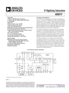
1 800 MHz Clock Distribution IC, Dividers, Delay Adjust, Three Outputs Data Sheet ad9513 . FEATURES FUNCTIONAL BLOCK DIAGRAM. RSET VS GND. GHz differential Clock input 3 programmable dividers ad9513 LVDS/CMOS. Divide-by in range from1 to 32 OUT0. /1.. /32. Phase select for coarse Delay adjust OUT0B. Three 800 MHz/250 MHz LVDS/CMOS Clock outputs Additive output jitter 300 fs rms LVDS/CMOS. Time delays up to ns CLK OUT1. /1.. /32. Device configured with 4-level logic pins CLKB OUT1B. Space-saving, 32-lead LFCSP. LVDS/CMOS. SYNCB. APPLICATIONS OUT2. /1.. /32 t Low jitter, low phase noise Clock Distribution OUT2B. Clocking high speed ADCs, DACs, DDSs, DDCs, DUCs, MxFEs High performance wireless transceivers SETUP LOGIC.
2 High performance instrumentation 05595-001. Broadband infrastructure VREF S10 S9 S8 S7 S6 S5 S4 S3 S2 S1 S0. ATE Figure 1. GENERAL DESCRIPTION. The ad9513 features a three-output Clock Distribution IC in a One of the outputs features a Delay element with three selectable design that emphasizes low jitter and phase noise to maximize full-scale Delay values ( ns, ns, and ns), each with data converter performance. Other applications with 16 steps of fine adjustment. demanding phase noise and jitter requirements also benefit The ad9513 does not require an external controller for from this part. operation or setup. The device is programmed by means of There are three independent Clock outputs that can be set to 11 pins (S0 to S10) using 4-level logic.
3 The programming pins either LVDS or CMOS levels. These outputs operate to are internally biased to VS. The VREF pin provides a level of 800 MHz in LVDS mode and to 250 MHz in CMOS mode. VS. VS ( V) and GND (0 V) provide the other two logic levels. Each output has a programmable divider that can be set to The ad9513 is ideally suited for data converter clocking divide by a selected set of integers ranging from 1 to 32. The applications where maximum converter performance is phase of one Clock output relative to the other Clock output can achieved by encode signals with subpicosecond jitter. be set by means of a divider phase select function that serves as The ad9513 is available in a 32-lead LFCSP and operates from a coarse timing adjustment.
4 A single V supply. The temperature range is 40 C to +85 C. Rev. B Document Feedback Information furnished by analog devices is believed to be accurate and reliable. However, no responsibility is assumed by analog devices for its use, nor for any infringements of patents or other rights of third parties that may result from its use. Specifications subject to change without notice. No One Technology Way, Box 9106, Norwood, MA 02062-9106, license is granted by implication or otherwise under any patent or patent rights of analog devices . Tel: 2005 2017 analog devices , Inc. All rights reserved. Trademarks and registered trademarks are the property of their respective owners.
5 Technical Support ad9513 Data Sheet TABLE OF CONTENTS. Features .. 1 Power-On SYNC .. 17. Applications .. 1 SYNCB .. 17. Functional Block Diagram .. 1 RSET Resistor .. 18. General Description .. 1 VREF .. 18. Revision History .. 2 Setup 18. 3 Divider Phase Offset .. 20. Clock Input .. 3 Delay Block .. 21. Clock Outputs .. 3 Outputs .. 21. Timing Characteristics .. 4 Power 22. Clock Output Phase Noise .. 6 Exposed Metal Paddle .. 22. Clock Output Additive Time Jitter .. 8 Power 22. SYNCB, VREF, and Setup Pins .. 9 Applications Information .. 23. Power .. 9 Using the ad9513 Outputs for ADC Clock Applications .. 23. Timing Diagrams .. 10 LVDS Clock Distribution .
6 23. Absolute Maximum Ratings .. 11 CMOS Clock Distribution .. 23. Thermal Characteristics .. 11. 1. Setup Pins (S0 to S10) .. 24. Pin Configuration and Function Descriptions .. 12 Power and Grounding Considerations and Power Supply Terminology .. 13 Rejection .. 24. Typical Performance Characteristics .. 14 Phase Noise and Jitter Measurement 25. Functional Description .. 17 Outline Dimensions .. 26. Overall .. 17 Ordering Guide .. 26. CLK, CLKB Differential Clock Input .. 17. Synchronization .. 17. REVISION HISTORY. 10/2017 Rev. A to Rev. B. Changed CP-32-7 to CP-32-2 .. Throughout Updated Outline Dimensions .. 26. Changes to Ordering Guide.
7 26. 1/2017 Rev. 0 to Rev. A. Changes to Figure 5 and Table 9 .. 12. Deleted Figure 6; Renumbered Sequentially .. 12. Change to Table 14 .. 19. Updated Outline Dimensions .. 26. Changes to Ordering Guide .. 26. 9/2005 Revision 0: Initial Version Rev. B | Page 2 of 28. Data Sheet ad9513 . SPECIFICATIONS. Typical (typ) is given for VS = V 5%; TA = 25 C, RSET = k , unless otherwise noted. Minimum (min) and maximum (max). values are given over full VS and TA ( 40 C to +85 C) variation. Clock INPUT. Table 1. Parameter Min Typ Max Unit Test Conditions/Comments Clock INPUT (CLK). Input Frequency 0 GHz Input Sensitivity 1 150 mV p-p Input Common-Mode Voltage, VCM V Self-biased; enables ac coupling Input Common-Mode Range, VCMR V With 200 mV p-p signal applied; dc-coupled Input Sensitivity, Single-Ended 150 mV p-p CLK ac-coupled; CLKB ac-bypassed to RF ground Input Resistance k Self-biased Input Capacitance 2 pF.
8 A slew rate of 1 V/ns is required to meet jitter, phase noise, and propagation Delay specifications. 1. Clock OUTPUTS. Table 2. Parameter Min Typ Max Unit Test Conditions/Comments LVDS Clock OUTPUT Termination = 100 differential Differential Output Frequency 0 800 MHz Differential Output Voltage (VOD) 250 350 450 mV. Delta VOD 30 mV. Output Offset Voltage (VOS) V. Delta VOS 25 mV. Short-Circuit Current (ISA, ISB) 14 24 mA Output shorted to GND. CMOS Clock OUTPUT Single-ended measurements; termination open Single-Ended Complementary output on (OUT1B). Output Frequency 0 250 MHz With 5 pF load Output Voltage High (VOH) VS V @ 1 mA load Output Voltage Low (VOL) V @ 1 mA load Rev.
9 B | Page 3 of 28. ad9513 Data Sheet TIMING CHARACTERISTICS. CLK input slew rate = 1 V/ns or greater. Table 3. Parameter Min Typ Max Unit Test Conditions/Comments LVDS Termination = 100 differential Output Rise Time, tRL 200 350 ps 20% to 80%, measured differentially Output Fall Time, tFL 210 350 ps 80% to 20%, measured differentially PROPAGATION Delay , tLVDS, CLK-TO-LVDS OUT Delay off on OUT2. OUT0, OUT1, OUT2. Divide = 1 ns Divide = 2 32 ns Variation with Temperature ps/ C. OUT2. Divide = 1 ns Divide = 2 32 ns Variation with Temperature ps/ C. OUTPUT SKEW, LVDS OUTPUTS Delay off on OUT2. OUT0 to OUT1 on Same Part, tSKV 1 135 20 +125 ps OUT0 to OUT2 on Same Part, tSKV1 205 65 +90 ps All LVDS OUTs Across Multiple Parts, tSKV_AB 2 375 ps Same LVDS OUTs Across Multiple Parts, tSKV_AB2 300 ps CMOS B outputs are inverted; termination = open Output Rise Time, tRC 650 865 ps 20% to 80%; CLOAD = 3 pF.
10 Output Fall Time, tFC 650 990 ps 80% to 20%; CLOAD = 3 pF. PROPAGATION Delay , tCMOS, CLK-TO-CMOS OUT Delay off on OUT2. OUT0, OUT1. Divide = 1 ns Divide = 2 32 ns Variation with Temperature 1 ps/ C. OUT2. Divide = 1 ns Divide = 2 32 ns Variation with Temperature 1 ps/ C. OUTPUT SKEW, CMOS OUTPUTS Delay off on OUT2. All CMOS OUTs on Same Part, tSKC1 230 +135 ps All CMOS OUTs Across Multiple Parts, tSKC_AB2 415 ps Same CMOS OUTs Across Multiple Parts, tSKC_AB2 330 ps LVDS-TO-CMOS OUT Everything the same; different logic type Output Skew, tSKV_C 510 ps LVDS to CMOS on same part Delay ADJUST (OUT2; LVDS AND CMOS). S0 = 1/3. Zero-Scale Delay Time 3 ns Zero-Scale Variation with Temperature ps/ C.