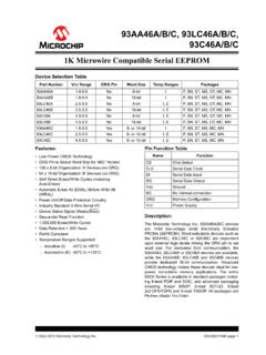
Transcription of 93AA66A/B/C, 93LC66A/B/C, 93C66A/B/C
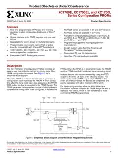
1 93aa66a /B/C, 93lc66a /B/C, 93C66A/B/C . 4K Microwire Compatible Serial EEPROM. Device Selection Table Part Number VCC Range ORG Pin Word Size Temp Ranges Packages 93aa66a No 8-bit I P, SN, ST, MS, OT, MC, MN. 93AA66B No 16-bit I P, SN, ST, MS, OT, MC, MN. 93lc66a No 8-bit I, E P, SN, ST, MS, OT, MC, MN. 93LC66B No 16-bit I, E P, SN, ST, MS, OT, MC, MN. 93c66a No 8-bit I, E P, SN, ST, MS, OT, MC, MN. 93C66B No 16-bit I, E P, SN, ST, MS, OT, MC, MN. 93AA66C Yes 8- or 16-bit I P, SN, ST, MS, MC, MN. 93LC66C Yes 8- or 16-bit I, E P, SN, ST, MS, MC, MN. 93C66C Yes 8- or 16-bit I, E P, SN, ST, MS, MC, MN. Features: Pin Function Table Low-Power CMOS Technology Name Function ORG Pin to Select Word Size for 66C' Version CS Chip Select 512 x 8-bit Organization A' Devices (no ORG) CLK Serial Data Clock 256 x 16-bit organization B' Devices (no ORG) DI Serial Data Input Self-tImed Erase/Write Cycles (including DO Serial Data Output Auto-Erase).
2 VSS Ground Automatic Erase All (ERAL) Before Write All (WRAL) NC No internal connection Power-On/Off Data Protection Circuitry ORG Memory Configuration Industry Standard 3-Wire Serial I/O VCC Power Supply Device Status Signal (Ready/Busy). Sequential Read Function Description: 1,000,000 Erase/Write Cycles The Microchip Technology Inc. 93XX66A/B/C devices Data Retention > 200 Years are 4 Kbit low-voltage serial Electrically Erasable Pb-free and RoHS Compliant PROMs (EEPROM). Word-selectable devices such as Temperature Ranges Supported: the 93AA66C, 93LC66C or 93C66C are dependent upon external logic levels driving the ORG pin to set - Industrial (I) -40 C to +85 C word size.
3 For dedicated 8-bit communication, the - Automotive (E) -40 C to +125 C 93XX66A devices are available, while the 93XX66B. devices provide dedicated 16-bit communication. Advanced CMOS technology makes these devices ideal for low-power, nonvolatile memory applications. The entire 93XX Series is available in standard packages including 8-lead PDIP and SOIC, and advanced packaging including 8-lead MSOP, 6-lead SOT-23, 8-lead 2x3 DFN/TDFN and 8-lead TSSOP. All packages are Pb-free (Matte Tin) finish. 2003-2011 Microchip Technology Inc. DS21795E-page 1. 93aa66a /B/C, 93lc66a /B/C, 93C66A/B/C . Package Types (not to scale). ROTATED SOIC PDIP/SOIC. (ex: 93LC46BX) (P, SN). NC 1 8 ORG* CS 1 8 VCC.
4 VCC 2 7 VSS CLK 2 7 NC. CS 3 6 DO DI 3 6 ORG*. CLK 4 5 DI DO 4 5 VSS. TSSOP/MSOP SOT-23. (ST, MS) (OT). CS 1 8 VCC DO 1 6 VCC. CLK 2 7 NC. DI 3 6 ORG* VSS 2 5 CS. DO 4 5 VSS. DI 3 4 CLK. DFN/TDFN. (MC, MN). CS 1 8 VCC. CLK 2 7 NC. DI 3 6 ORG*. DO 4 5 VSS. *ORG pin is NC on A/B devices. DS21795E-page 2 2003-2011 Microchip Technology Inc. 93aa66a /B/C, 93lc66a /B/C, 93C66A/B/C . ELECTRICAL CHARACTERISTICS. Absolute Maximum Ratings( ). All inputs and outputs VSS .. to VCC + Storage temperature ..-65 C to +150 C. Ambient temperature with power C to +125 C. ESD protection on all pins 4 kV. NOTICE: Stresses above those listed under Absolute Maximum Ratings may cause permanent damage to the device.
5 This is a stress rating only and functional operation of the device at those or any other conditions above those indicated in the operational listings of this specification is not implied. Exposure to maximum rating conditions for extended periods may affect device reliability. TABLE 1-1: DC CHARACTERISTICS. All parameters apply over the specified Industrial (I): TA = -40 C to +85 C, VCC = + to + ranges unless otherwise noted. Automotive (E): TA = -40 C to +125 C, VCC = + to + Param. Symbol Parameter Min Typ Max Units Conditions No. D1 VIH1 High-level input voltage VCC +1 V VCC VIH2 VCC VCC +1 V VCC < D2 VIL1 Low-level input voltage V VCC VIL2 VCC V VCC < D3 VOL1 Low-level output voltage V IOL = mA, VCC = VOL2 V IOL = 100 A, VCC = D4 VOH1 High-level output voltage V IOH = -400 A, VCC = VOH2 VCC - V IOH = -100 A, VCC = D5 ILI Input leakage current 1 A VIN = VSS or VCC.
6 D6 ILO Output leakage current 1 A VOUT = VSS or VCC. D7 CIN, Pin capacitance (all inputs/ 7 pF VIN/VOUT = 0V (Note 1). COUT outputs) TA = 25 C, FCLK = 1 MHz D8 ICC write Write current 2 mA FCLK = 3 MHz, Vcc = 500 A FCLK = 2 MHz, Vcc = D9 ICC read Read current 1 mA FCLK = 3 MHz, VCC = 500 A FCLK = 2 MHz, VCC = 100 A FCLK = 2 MHz, VCC = D10 ICCS Standby current 1 A I Temp 5 A E Temp CLK = Cs = 0V. ORG = DI = VSS or VCC. (Note 2) (Note 3). D11 VPOR VCC voltage detect 93aa66a /B/C, 93lc66a /B/C V (Note 1). 93C66A/B/C V. Note 1: This parameter is periodically sampled and not 100% tested. 2: ORG pin not available on A' or B' versions. 3: Ready/Busy status must be cleared from DO; see Section "Data Out (DO)".
7 2003-2011 Microchip Technology Inc. DS21795E-page 3. 93aa66a /B/C, 93lc66a /B/C, 93C66A/B/C . TABLE 1-2: AC CHARACTERISTICS. All parameters apply over the specified Industrial (I): TA = -40 C to +85 C, VCC = + to + ranges unless otherwise noted. Automotive (E): TA = -40 C to +125 C, VCC = + to + Param. Symbol Parameter Min Max Units Conditions No. A1 FCLK Clock frequency 3 MHz VCC < , 93XX66C only 2 MHz VCC < 1 MHz VCC < A2 TCKH Clock high time 200 ns VCC < , 93XX66C only 250 ns VCC < 450 ns VCC < A3 TCKL Clock low time 100 ns VCC < , 93XX66C only 200 ns VCC < 450 ns VCC < A4 TCSS Chip Select setup time 50 ns VCC < 100 ns VCC < 250 ns VCC < A5 TCSH Chip Select hold time 0 ns VCC < A6 TCSL Chip Select low time 250 ns VCC < A7 TDIS Data input setup time 50 ns VCC < , 93XX66C only 100 ns VCC < 250 ns VCC < A8 TDIH Data input hold time 50 ns VCC < , 93XX66C only 100 ns VCC < 250 ns VCC < A9 TPD Data output delay time 200 ns VCC < , CL = 100 pF.
8 250 ns VCC < , CL = 100 pF. 400 ns VCC < , CL = 100 pF. A10 TCZ Data output disable time 100 ns VCC < , (Note 1). 200 ns VCC < , (Note 1). A11 TSV Status valid time 200 ns VCC < , CL = 100 pF. 300 ns VCC < , CL = 100 pF. 500 ns VCC < , CL = 100 pF. A12 TWC Program cycle time 6 ms Erase/Write mode (AA and LC. versions). A13 TWC 2 ms Erase/Write mode (93C versions). A14 TEC 6 ms ERAL mode, VCC A15 TWL 15 ms WRAL mode, VCC A16 Endurance 1M cycles 25 C, VCC = , (Note 2). Note 1: This parameter is periodically sampled and not 100% tested. 2: This application is not tested but ensured by characterization. For endurance estimates in a specific application, please consult the Total Endurance Model, which may be obtained from Microchip's web site at DS21795E-page 4 2003-2011 Microchip Technology Inc.
9 93aa66a /B/C, 93lc66a /B/C, 93C66A/B/C . FIGURE 1-1: SYNCHRONOUS DATA TIMING. VIH. CS. VIL TCSS TCKH TCKL. TCSH. VIH. CLK. VIL. TDIS TDIH. VIH. DI. VIL. TPD TCZ. TPD. VOH. DO. (Read) TCZ. VOL. TSV. DO VOH. (Program) Status Valid VOL. Note: TSV is relative to CS. TABLE 1-3: INSTRUCTION SET FOR X16 ORGANIZATION (93XX66B OR 93XX66C WITH ORG = 1). Instruction SB Opcode Address Data In Data Out Req. CLK Cycles ERASE 1 11 A7 A6 A5 A4 A3 A2 A1 A0 (RDY/BSY) 11. ERAL 1 00 1 0 X X X X X X (RDY/BSY) 11. EWDS 1 00 0 0 X X X X X X High-Z 11. EWEN 1 00 1 1 X X X X X X High-Z 11. READ 1 10 A7 A6 A5 A4 A3 A2 A1 A0 D15 D0 27. WRITE 1 01 A7 A6 A5 A4 A3 A2 A1 A0 D15 D0 (RDY/BSY) 27. WRAL 1 00 0 1 X X X X X X D15 D0 (RDY/BSY) 27.
10 TABLE 1-4: INSTRUCTION SET FOR X8 ORGANIZATION (93XX66A OR 93XX66C WITH ORG = 0). Req. CLK. Instruction SB Opcode Address Data In Data Out Cycles ERASE 1 11 A8 A7 A6 A5 A4 A3 A2 A1 A0 (RDY/BSY) 12. ERAL 1 00 1 0 X X X X X X X (RDY/BSY) 12. EWDS 1 00 0 0 X X X X X X X High-Z 12. EWEN 1 00 1 1 X X X X X X X High-Z 12. READ 1 10 A8 A7 A6 A5 A4 A3 A2 A1 A0 D7 D0 20. WRITE 1 01 A8 A7 A6 A5 A4 A3 A2 A1 A0 D7 D0 (RDY/BSY) 20. WRAL 1 00 0 1 X X X X X X X D7 D0 (RDY/BSY) 20. 2003-2011 Microchip Technology Inc. DS21795E-page 5. 93aa66a /B/C, 93lc66a /B/C, 93C66A/B/C . FUNCTIONAL DESCRIPTION Data In/Data Out (DI/DO). When the ORG pin is connected to VCC, the (x16) orga- It is possible to connect the Data In and Data Out pins nization is selected.