Transcription of a 16-Channel, 8-Bit Multiplying DAC AD8600 - …
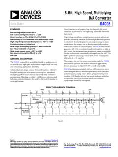
1 One Technology Way, Box 9106, Norwood. MA 02062-9106, : 617/329-4700 Fax: 617/326-8703 FUNCTIONAL BLOCK DIAGRAMR/W VDD1 LDCONTROL LOGIC ADDRESSDECODE16 x 8 INPUTREGISTERSRS VDD2 VREFVCC16 x 8 DACREGISTERS168-BITDACSCS EN A3A2A1A0 DB7DB6DB5DB4DB3DB2DB1DB0O0O1O2O3O4O5O6O7 O8O9O10O11O12O13O14O15 VEEDGND1 DGND2 DACGNDAD8600 REV. 0 Information furnished by Analog Devices is believed to be accurate andreliable. However, no responsibility is assumed by Analog Devices for itsuse, nor for any infringements of patents or other rights of third partieswhich may result from its use. No license is granted by implication orotherwise under any patent or patent rights of Analog , 8-BitMultiplying DACAD8600 FEATURES16 Independently Addressable Voltage OutputsFull-Scale Set by External Reference2 s Settling TimeDouble Buffered 8-Bit Parallel InputHigh Speed Data Load RateData ReadbackOperates from Single +5 VOptional 6 V Supply Extends Output RangeAPPLICATIONSP hased Array Ultrasound & SonarPower Level SettingReceiver Gain SettingAutomatic Test EquipmentLCD Clock Level SettingGENERAL DESCRIPTIONThe AD8600 contains 16 independent voltage output digital-to-analog converters that share a common external reference inputvoltage.
2 Each DAC has its own DAC register and input registerto allow double buffering. An 8-Bit parallel data input, four ad-dress pins, a CS select, a LD, EN, R/W, and RS provide thedigital AD8600 is constructed in a monolithic CBCMOS processwhich optimizes use of CMOS for logic and bipolar for speedand precision. The digital-to-analog converter design uses volt-age mode operation ideally suited to single supply internal DAC voltage range is fixed at DACGND to voltage buffers provide an output voltage range that ap-proaches ground and extends to V below VCC. Changes inreference voltage values and digital inputs will settle within 1 LSB in 2 is preloaded into the input registers one at a time after theinternal address decoder selects the input register. In the writemode (R/W low) data is latched into the input register duringthe positive edge of the EN pulse. Pulses as short as 40 ns canbe used to load the data.
3 After changes have been submitted tothe input registers, the DAC registers are simultaneously up-dated by a common load EN LD strobe. The new analog out-put voltages simultaneously appear on all 16 system power up or during fault recovery the reset (RS) pinforces all DAC registers into the zero state which places zerovolts at all DAC AD8600 is offered in the PLCC-44 package. The device isdesigned and tested for operation over the extended industrialtemperature range of 40 C to +85 CS ADDRESS RS VDD2 VREFVCCDGND2 DGND1R-2 RDAC LD ENVEERSR/W CS ADDR EN 1. Equivalent DAC Channel AD8600 SPECIFICATIONSSINGLE SUPPLYP arameterSymbolConditionMinTypMaxUnitsSTA TIC PERFORMANCE1 ResolutionN8 BitsRelative Accuracy2 INL 1 1/2+1 LSBD ifferential Nonlinearity2 DNLG uaranteed Monotonic 1 1/4+1 LSBFull-Scale VoltageVFSData = TempcoTCVFSData = FFH 20ppm/ CZero Scale ErrorVZSEData = 00H, RS = 0, TA= +25 C+ = 00H, RS = 0 +5 LSBR eference Input ResistanceRREFData = ANALOG OUTPUTO utput Voltage Range2 OVRSSVREF = + CurrentIOUTData = 80H 2mACapacitive LoadCLNo Oscillation50pFLOGIC INPUTSL ogic Input Low Input High Input CurrentIIL10 ALogic Input Capacitance3 CIL10pFLOGIC OUTPUTSL ogic Out High VoltageVOHIOH = Out Low VoltageVOLIOL = CHARACTERISTICS3 Slew RateSRFor VREF or FS Code Change47V/ sVoltage Output Settling Time2tS1 1 LSB of Final Value.
4 Full-Scale Data Change2 sVoltage Output Settling Time2tS2 1 LSB of Final Value, VREF = 1 V, Data = FFH2 sPOWER SUPPLIESP ositive Supply CurrentICCVIH = 5 V, VIL = 0 V, No Load2435mALogic Supply CurrentsIDD1&2 VIH = 5 V, VIL = 0 V, No DissipationPDISSVIH = 5 V, VIL = 0 V, No Load120175mWPower Supply SensitivityPSS VCC = 5% Power Supply Power Supply VREF = V, 1 LSB = supply operation does not include the final 2 LSBs near analog ground. If this performance is critical, use a negative supply (VEE) pin of at least V to V. Note that for the INL measurement zero-scale voltage is extrapolated using codes 710 to by design not subject to production subject to change without 0 2 (@ VDD1 = VDD2 = VCC = +5 V 5%, VEE = 0 V, VREF = + V, 40 C TA +85 C, unless otherwise noted)ParameterSymbolConditionMinTypMaxU nitsSTATIC PERFORMANCE1 ResolutionN8 BitsTotal Unadjusted ErrorTUEAll Other DACs Loaded with Data = 55H 1 3/4+1 LSBR elative AccuracyINL 1 1/2+1 LSBD ifferential NonlinearityDNLG uaranteed Monotonic 1 1/4+1 LSBFull-Scale VoltageVFSData = FFH, VREF = + Voltage ErrorVFSEData = FFH, VREF = + V 1+1 LSBFull-Scale TempcoTCVFSData = FFH, VREF = + V 20ppm/ CZero Scale ErrorVZSEData = 00H, RS = 0, TA = +25 C 2 1+2 mVZero Scale ErrorVZSEData = 00H, All Other DACs Data = 00H 1+1 LSBZero Scale ErrorVZSEData = 00H, All Other DACs Data = 55H 1/2 LSBZero Scale TempcoTCVZSData = 00H, VCC = +5 V, VEE = 5 V 10 V/ CReference Input ResistanceRREFData = Reference Input Capacitance2 CREFData = ABH240pFANALOG OUTPUTO utput Voltage RangeOVR1 VREF = + Voltage Range2 OVR2 VCC = VDD2 = +7 V, VEE = V.
5 VREF = 5 CurrentIOUTData = 80H 2mACapacitive Load2 CLNo Oscillation50pFLOGIC INPUTSL ogic Input Low Input High Input CurrentIIL10 ALogic Input Capacitance2 CIL10pFLOGIC OUTPUTSL ogic Out High VoltageVOHIOH = Out Low VoltageVOLIOL = CHARACTERISTICS2 Reference In BandwidthBW 3 dB Frequency, VREF = VDC + VAC500kHzSlew RateSRFor VREF or FS Code Change47V/ sVoltage Noise DensityeNf = 1 kHz, VREF = 0 V46nV/ HzDigital FeedthroughFTDigital Inputs to DAC Outputs10nVsVoltage Output Settling Time3tS1 1 LSB of Final Value, FS Data Change12 sVoltage Output Settling Time3tS2 1 LSB of Final Value, VREF = 1 V, Data = FFH12 sPOWER SUPPLIESP ositive Supply CurrentICCVIH = 5 V, VIL = 0 V, VEE = 5 V, No Load2235mANegative Supply CurrentIEEVIH = 5 V, VIL = 0 V, VEE = 5 V, No Load2235mALogic Supply CurrentsIDD1&2 VIH = 5 V, VIL = 0 V, VEE = 5 V, No Dissipation4 PDISSVIH = 5 V, VIL = 0 V, VEE = 5 V, No Load225350mWPower Supply SensitivityPSS VCC & VEE = 5% Power Supply Power Supply Power Supply Range2 VEER VREF = + V, 1 LSB = by design not subject to production time test is performed using RL = 50 k and CL = 35 Dissipation is calculated using 5 V (IDD + |ISS| + IDD1 + IDD2).
6 Specifications subject to change without SUPPLY(@ VDD1 = VDD2 = VCC = +5 V 5%, VEE = 5 V 5%, VREF = + V, 40 C TA +85 C, unless otherwise noted) AD8600 REV. 0 3 REV. 0 4 AD8600 ELECTRICAL CHARACTERISTICSP arameterSymbolConditionMinTypMaxUnitsINT ERFACE TIMING1, 2 Clock (EN) FrequencyfCLKData (EN) High Pulse WidthtCH40nsClock (EN) LowPulse WidthtCL40nsData Setup TimetDS40nsData Hold TimetDH10nsAddress Setup TimetAS0nsAddress Hold TimetAH0nsValid Address to Data ValidtAD160nsLoad Enable Setup TimetLS0nsLoad Enable Hold TimetLH0nsRead/Write to Clock (EN)tRWC30nsRead/Write to DataBus Hi-ZtRWZ120nsRead/Write to DataBus ActivetRWD120nsClock (EN) to Read/WritetTWH0nsClock (EN) to Chip SelecttTCH0nsChip Select to Clock (EN)tCSC30nsChip Select to Data ValidtCSD120nsChip Select to DataBus Hi-ZtCSZ150nsReset Pulse WidthtRS25nsNOTES1 Guaranteed by design not subject to production logic input signals have maximum rise and fall times of 2 subject to change without 3.
7 Readback TimingFigure 2. Write Timing(@ VDD1 = VDD2 = VCC = +5 V 5%, VEE = 5 V, VREF = + V, 40 C TA +85 C,unless otherwise noted)tRWZtDHtTWHHIGH-ZtAStAHtCHtCLtTCHR /WDATAADDRENCStCSCtRWCtDSFigure 4. Write to DAC Register & Voltage Output SettlingTiming (CS= High, Prevents Input Register Changes)tLStLHtS1tRSOUTtS1 ENRSLDtRWDHIGH -ZtADtCSZtCSDR/WDATAADDRENCSAD8600 REV. 0 5 PIN DESCRIPTIONPin Connection2 VREFR eference input voltage commonto all Analog Ground Return. Sets analog zero-scale Amplifier Positive Supply5 VEEO utput Amplifier Negative Supply6O7 DAC Channel Output No. 77O6 DAC Channel Output No. 68O5 DAC Channel Output No. 59O4 DAC Channel Output No. 410O3 DAC Channel Output No. 311O2 DAC Channel Output No. 212O1 DAC Channel Output No. 113O0 DAC Channel Output No. 014 VDD1 Digital Logic Power Supply15 RSActive Low Reset Input Pin16DB0 Data Bit Zero I/O (LSB)17DB1 Data Bit I/O18DB2 Data Bit I/O19DB3 Data Bit I/O20DB4 Data Bit I/O21DB5 Data Bit I/O22DB6 Data Bit I/O23DB7 Most Significant Data Bit I/O (MSB)24A0 Address Bit Zero (LSB)25A1 Address Bit26A2 Address Bit27A3 Most Significant Addr Bit (MSB)28R/WRead/Write Select Control Input29 ENActive Low Enable Clock Strobe30 CSChip Select Input31 LDDAC Register Load Strobe32 DGND1 Digital Ground Input No.
8 133O15 DAC Channel Output No. 1534O14 DAC Channel Output No. 1435O13 DAC Channel Output No. 1336O12 DAC Channel Output No. 1237O11 DAC Channel Output No. 1138O10 DAC Channel Output No. 1039O9 DAC Channel Output No. 940O8 DAC Channel Output No. 841 VEEO utput Amplifier Negative Supply42 VCCO utput Amplifier Positive Supply43 DGND2 Digital Ground Input No. 244 VDD2 DAC Analog Supply VoltageWARNING!ESD SENSITIVE DEVICECAUTIONESD (electrostatic discharge) sensitive device. Electrostatic charges as high as 4000 V readilyaccumulate on the human body and test equipment and can discharge without the AD8600 features proprietary ESD protection circuitry, permanent damage mayoccur on devices subjected to high energy electrostatic discharges. Therefore, proper ESDprecautions are recommended to avoid performance degradation or loss of MAXIMUM RATINGS(TA= +25 C unless otherwise noted)VDD1 (Digital Supply) to GND.
9 V, +7 VVDD2 (DAC Buffer/Driver Supply) .. V, +7 VVCC (Analog Supply) to GND .. V, +7 VVEE (Analog Supply) to GND .. + V, 7 VVREF to GND .. V, VCC + VVDD2 to VREF .. VVOUT to GND .. VCCS hort Circuit DurationVOUT to GND or Power Supplies1 ..ContinuousDigital Input/Output Voltage to GND .. V, VDD + VThermal Resistance Theta Junction-to-Ambient ( JA)PLCC-44 .. 47 C/WPackage Power Dissipation .. (TJ TA)/ JAMaximum Junction Temperature TJ max .. 150 COperating Temperature Range .. 40 C to +85 CStorage Temperature Range .. 65 C to +150 CLead Temperature (Soldering, 10 sec) .. +300 CNOTE1No more than four outputs may be shorted to power or GND CONFIGURATIONNC = NO CONNECTO9O10O13O14O15O11O12O6O5O2O1O0O4O 3O7 VEEVREFNCVDD2 VCCDB2DB3DB6DB7A0DB4DB5 DACGNDVCCVEEO8A2A3R/WA1 DGND2 LDCSENDGND1 RSDB0DB1 VDD1441264521242322182019393835343337363 7811121391040414225282726433130293215161 714 TOP VIEW(Not to Scale) AD8600 ORDERING GUIDEP ackagePackageModelTemperatureDescription OptionAD8600AP 40 C to +85 C 44-Lead PLCCP-44 AAD8600 Chips+25 CDie**For die specifications contact your local Analog Devices sales AD8600 contains 5782 0 6 AD8600 TRANSFER EQUATIONSO utput Voltage Oi=D VREF256where i is the DAC channel number and D is the decimal valueof the DAC register I.
10 Truth TableENR/WCSLDRSO perationWrite to DAC Register XHLHU pdate DAC RegisterLXH HUpdate DAC Register+XHLHL atches DAC RegisterLXH+HLatches DAC RegisterLLLLHDAC Register TransparentWrite to Input RegisterLLLHHLoad Data to Input Register atDecoded Address+LLHHL atches Data in Input Register atDecoded AddressLL+HHLatches Data in Input Register atDecoded AddressReadback Input RegistersXHLHHI nput Register Readback (DataAccess)XH+HHHi-Z Readback Disconnects fromBusXXHXXHi-Z on Data BusResetXXXXLC lear All Registers to Zero,VOUT = 0 VXXHH+Latches All Registers to ZeroLX LH +CS = Low; Input Register Readyfor R/W, DAC Register Latchedto ZeroNOTES1+ symbol means positive edge of control input symbol means negative edge of control input DAC Register Oi=Awhere A is the decimal value of the decoded address bits A3,A2, A1, A0 (LSB).Address, CS, R/W and data inputs should be stable prior to acti-vation of the active low EN input.