Transcription of a Instrumentation Amplifier Precision AD624 - analog.com
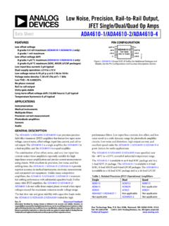
1 A Precision Instrumentation Amplifier AD624 . FEATURES FUNCTIONAL BLOCK DIAGRAM. Low Noise: V p-p Hz to 10 Hz Low Gain TC: 5 ppm max (G = 1) 50 . INPUT. Low Nonlinearity: max (G = 1 to 200). High CMRR: 130 dB min (G = 500 to 1000) G = 100. AD624 . Low Input Offset Voltage: 25 V, max . Low Input Offset Voltage Drift: V/ C max G = 200 . 124 . Gain Bandwidth Product: 25 MHz VB 10k . G = 500 SENSE. Pin Programmable Gains of 1, 100, 200, 500, 1000 . 20k 10k . No External Components Required RG1. 20k 10k OUTPUT. Internally Compensated RG2. 10k . REF. 50 . +INPUT. PRODUCT DESCRIPTION PRODUCT HIGHLIGHTS. The AD624 is a high Precision , low noise, Instrumentation 1. The AD624 offers outstanding noise performance. Input Amplifier designed primarily for use with low level transducers, noise is typically less than 4 nV/ Hz at 1 kHz. including load cells, strain gauges and pressure transducers.
2 An 2. The AD624 is a functionally complete Instrumentation am- outstanding combination of low noise, high gain accuracy, low plifier. Pin programmable gains of 1, 100, 200, 500 and 1000. gain temperature coefficient and high linearity make the AD624 are provided on the chip. Other gains are achieved through ideal for use in high resolution data acquisition systems. the use of a single external resistor. The AD624C has an input offset voltage drift of less than 3. The offset voltage, offset voltage drift, gain accuracy and gain V/ C, output offset voltage drift of less than 10 V/ C, temperature coefficients are guaranteed for all pretrimmed CMRR above 80 dB at unity gain (130 dB at G = 500) and a gains. maximum nonlinearity of at G = 1. In addition to these outstanding dc specifications, the AD624 exhibits superior ac 4. The AD624 provides totally independent input and output performance as well.
3 A 25 MHz gain bandwidth product, 5 V/ s offset nulling terminals for high Precision applications. slew rate and 15 s settling time permit the use of the AD624 in This minimizes the effect of offset voltage in gain ranging high speed data acquisition applications. applications. The AD624 does not need any external components for pre- 5. A sense terminal is provided to enable the user to minimize trimmed gains of 1, 100, 200, 500 and 1000. Additional gains the errors induced through long leads. A reference terminal is such as 250 and 333 can be programmed within one percent also provided to permit level shifting at the output. accuracy with external jumpers. A single external resistor can also be used to set the 624's gain to any value in the range of 1. to 10,000. REV. C. Information furnished by analog Devices is believed to be accurate and reliable.
4 However, no responsibility is assumed by analog Devices for its use, nor for any infringements of patents or other rights of third parties One Technology Way, Box 9106, Norwood, MA 02062-9106, which may result from its use. No license is granted by implication or Tel: 781/329-4700 otherwise under any patent or patent rights of analog Devices. Fax: 781/326-8703 analog Devices, Inc., 1999. AD624 SPECIFICATIONS (@ V = 15 V, R = 2 k and T = +25 C, unless otherwise noted). S L A. Model AD624A AD624B AD624C AD624S. Min Typ Max Min Typ Max Min Typ Max Min Typ Max Units GAIN. Gain Equation (External Resistor Gain Programming) 40, 000 40, 000 40, 000 40, 000 . R + 1 20% R + 1 20% R + 1 20% R + 1 20%. G G G G . Gain Range (Pin Programmable) 1 to 1000 1 to 1000 1 to 1000 1 to 1000. Gain Error G=1 %. G = 100 %. G = 200, 500 %. Nonlinearity G=1 %.
5 G = 100, 200 %. G = 500 %. Gain vs. Temperature G=1 5 5 5 5 ppm/ C. G = 100, 200 10 10 10 10 ppm/ C. G = 500 25 15 15 15 ppm/ C. VOLTAGE OFFSET (May be Nulled). Input Offset Voltage 200 75 25 75 V. vs. Temperature 2 V/ C. Output Offset Voltage 5 3 2 3 mV. vs. Temperature 50 25 10 50 V/ C. OUT. Offset Referred to the Input vs. Supply G=1 70 75 80 75 dB. G = 100, 200 95 105 110 105 dB. G = 500 100 110 115 110 dB. INPUT CURRENT. Input Bias Current 50 25 15 50 nA. vs. Temperature 50 50 50 50 pA/ C. Input Offset Current 35 15 10 35 nA. vs. Temperature 20 20 20 20 pA/ C. INPUT. Input Impedance Differential Resistance 109 109 109 109 . Differential Capacitance 10 10 10 10 pF. Common-Mode Resistance 109 109 109 109 . Common-Mode Capacitance 10 10 10 10 pF. Input Voltage Range1. Max Differ. Input Linear (VDL) 10 10 10 10 V. G G G G . Max Common-Mode Linear (V CM) 12 V 2 VD 12 V 2 VD 12 V 2 VD 12 V 2 VD V.
6 Common-Mode Rejection dc to 60 Hz with 1 k Source Imbalance G=1 70 75 80 70 dB. G = 100, 200 100 105 110 100 dB. G = 500 110 120 130 110 dB. OUTPUT RATING. V , RL = 2 k 10 10 10 10 V. DYNAMIC RESPONSE. Small Signal 3 dB. G=1 1 1 1 1 MHz G = 100 150 150 150 150 kHz G = 200 100 100 100 100 kHz G = 500 50 50 50 50 kHz G = 1000 25 25 25 25 kHz Slew Rate V/ s Settling Time to , 20 V Step G = 1 to 200 15 15 15 15 s G = 500 35 35 35 35 s G = 1000 75 75 75 75 s NOISE. Voltage Noise, 1 kHz 4 4 4 4 nV/ Hz 75 75 75 75 nV/ Hz , Hz to 10 Hz G=1 10 10 10 10 V p-p G = 100 V p-p G = 200, 500, 1000 V p-p Current Noise Hz to 10 Hz 60 60 60 60 pA p-p SENSE INPUT. RIN 8 10 12 8 10 12 8 10 12 8 10 12 k . IIN 30 30 30 30 A. Voltage Range 10 10 10 10 V. Gain to Output 1 1 1 1 %. 2 REV. C. AD624 . Model AD624A AD624B AD624C AD624S. Min Typ Max Min Typ Max Min Typ Max Min Typ Max Units REFERENCE INPUT.
7 RIN 16 20 24 16 20 24 16 20 24 16 20 24 k . IIN 30 30 30 30 A. Voltage Range 10 10 10 10 V. Gain to Output 1 1 1 1 %. TEMPERATURE RANGE. Specified Performance 25 +85 25 +85 25 +85 55 +125 C. Storage 65 +150 65 +150 65 +150 65 +150 C. POWER SUPPLY. Power Supply Range 6 15 18 6 15 18 6 15 18 6 15 18 V. Quiescent Current 5 5 5 5 mA. NOTES. 1. VDL is the maximum differential input voltage at G = 1 for specified nonlinearity, V DL at other gains = 10 V/G. V D = actual differential input voltage. 1. Example: G = 10, V D = VCM = 12 V (10/2 V) = V. Specifications subject to change without notice. Specifications shown in boldface are tested on all production unit at final electrical test. Results from those tests are used to calculate outgoing quality levels. All min and max specifications are guaranteed, although only those shown in boldface are tested on all production units.
8 ABSOLUTE MAXIMUM RATINGS* CONNECTION DIAGRAM. Supply Voltage .. 18 V. Internal Power Dissipation .. 420 mW. Input Voltage .. VS INPUT 1 16 RG1. Differential Input Voltage .. VS +INPUT 2 15 OUTPUT NULL. Output Short Circuit Duration .. Indefinite RG2 3 14 OUTPUT NULL. Storage Temperature Range .. 65 C to +150 C INPUT NULL 4 AD624 13 G = 100 SHORT TO. TOP VIEW. Operating Temperature Range INPUT NULL 5 (Not to Scale) 12 G = 200. RG2 FOR. DESIRED. AD624A/B/C .. 25 C to +85 C REF 6 11 G = 500 GAIN. AD624S .. 55 C to +125 C VS 7 10 SENSE. Lead Temperature (Soldering, 60 secs) .. +300 C +VS 8 9 OUTPUT. *Stresses above those listed under Absolute Maximum Ratings may cause perma- nent damage to the device. This is a stress rating only; functional operation of the FOR GAINS OF 1000 SHORT RG1 TO PIN 12. device at these or any other conditions above those indicated in the operational AND PINS 11 AND 13 TO RG2.
9 Sections of this specification is not implied. Exposure to absolute maximum rating conditions for extended periods may affect device reliability. METALIZATION PHOTOGRAPH. Contact factory for latest dimensions ORDERING GUIDE Dimensions shown in inches and (mm). Temperature Package Package Model Range Description Option AD624AD 25 C to +85 C 16-Lead Ceramic DIP D-16. AD624BD 25 C to +85 C 16-Lead Ceramic DIP D-16. AD624CD 25 C to +85 C 16-Lead Ceramic DIP D-16. AD624SD 55 C to +125 C 16-Lead Ceramic DIP D-16. AD624SD/883B* 55 C to +125 C 16-Lead Ceramic DIP D-16. AD624 AChips 25 C to +85 C Die AD624 SChips 25 C to +85 C Die *See analog Devices' military data sheet for 883B specifications. REV. C 3 . AD624 Typical Characteristics 20 20 30. OUTPUT VOLTAGE SWING V p-p OUTPUT VOLTAGE SWING V. INPUT VOLTAGE RANGE V. 15 15. 20. +25 C.
10 10 10. 10. 5 5. 0 0 0. 0 5 10 15 20 0 5 10 15 20 10 100 1k 10k SUPPLY VOLTAGE V SUPPLY VOLTAGE V LOAD RESISTANCE . Figure 1. Input Voltage Range vs. Figure 2. Output Voltage Swing vs. Figure 3. Output Voltage Swing vs. Supply Voltage, G = 1 Supply Voltage Load Resistance 16 40. Amplifier QUIESCENT CURRENT mA. 14 30. INPUT BIAS CURRENT nA. INPUT BIAS CURRENT nA. 12 20. 10 10. 8 0. 6 10. 4 20. 2 30. 0 0 40. 0 5 10 15 20 0 5 10 15 20 125 75 25 25 75 125. SUPPLY VOLTAGE V SUPPLY VOLTAGE V TEMPERATURE C. Figure 4. Quiescent Current vs. Figure 5. Input Bias Current vs. Figure 6. Input Bias Current vs. Supply Voltage Supply Voltage Temperature 16. 1. 14. 0. VOS FROM FINAL VALUE V. INPUT BIAS CURRENT nA. 12. 1. 500. 10. GAIN V/V. 2 100. 8. 3 10. 6. 4. 1. 4. 5. 2. 6. 0 0. 0 5 10 15 20 7 1 10 100 1k 10k 100k 1M 10M. 0 INPUT VOLTAGE V FREQUENCY Hz WARM-UP TIME Minutes Figure 7.