Transcription of a Low Noise, Precision, High Speed Operational …
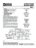
1 REV. BInformation furnished by Analog Devices is believed to be accurate andreliable. However, no responsibility is assumed by Analog Devices for itsuse, nor for any infringements of patents or other rights of third parties thatmay result from its use. No license is granted by implication or otherwiseunder any patent or patent rights of Analog Technology Way, Box 9106, Norwood, MA 02062-9106, : 781/329-4700 : 781/326-8703 Analog Devices, Inc., 2002 Low noise , Precision, high SpeedOperational Amplifier (A VCL > 5)SIMPLIFIED SCHEMATICV V+Q2BR2*Q3Q2AQ1AQ1BR4R1*R318 VOS AND R2 ARE PERMANENTLYADJUSTED AT WAFER TEST FORMINIMUM OFFSET VOLTAGE.
2 *NON-INVERTINGINPUT (+)INVERTINGINPUT ( )Q6Q21C2R23R24Q23Q24Q22R5Q11 Q12Q27Q28C1R9R12C3C4Q26Q20Q19Q46Q45 OUTPUTFEATURESLow noise , 80 nV p-p ( Hz to 10 Hz)3 nV/ Hz @ 1 kHzLow Drift, V/ CHigh Speed , 17 V/ s Slew Rate63 MHz Gain BandwidthLow Input Offset Voltage, 10 VExcellent CMRR, 126 dB (Common-Voltage @ 11 V) high Open-Loop Gain, MillionReplaces 725, OP-07, SE5534 In Gains > 5 Available in Die FormGENERAL DESCRIPTIONThe OP37 provides the same high performance as the OP27,but the design is optimized for circuits with gains greater thanfive. This design change increases slew rate to 17 V/ms andgain-bandwidth product to 63 OP37 provides the low offset and drift of the OP07plus higher Speed and lower noise .
3 Offsets down to 25 mV anda maximum drift of mV/ C make the OP37 ideal for preci-sion instrumentation applications. Exceptionally low noise (en= nV/ @ 10 Hz), a low 1/f noise corner frequency Hz, and the high gain of million, allow accuratehigh-gain amplification of low-level low input bias current of 10 nA and offset current of 7 nAare achieved by using a bias-current cancellation circuit. Overthe military temperature range this typically holds IB and IOSto 20 nA and 15 nA CONNECTIONS8-Lead Hermetic DIP(Z Suffix)Epoxy Mini-DIP(P Suffix)8-Lead SO(S Suffix)87651234NC = NO CONNECTVOS TRIM IN+INVOS TRIMV+OUTNCV OP37 The output stage has good load driving capability.
4 A guaranteedswing of 10 V into 600 W and low output distortion make theOP37 an excellent choice for professional audio and CMRR exceed 120 dB. These characteristics, coupledwith long-term drift of mV/month, allow the circuit designerto achieve performance levels previously attained only bydiscrete , high -volume production of the OP37 is achieved byusing on-chip zener-zap trimming. This reliable and stable offsettrimming scheme has proved its effectiveness over many years ofproduction OP37 brings low- noise instrumentation-type performance tosuch diverse applications as microphone, tapehead, and RIAA phono preamplifiers, high - Speed signal conditioning for dataacquisition systems, and wide-bandwidth BOP37 2 ABSOLUTE MAXIMUM RATINGS4 Supply Voltage.
5 22 VInternal Voltage (Note 1 ) .. 22 VOutput Short-Circuit Duration .. IndefiniteDifferential Input Voltage (Note2) .. VDifferential Input Current (Note 2) .. 25 mAStorage Temperature Range .. 65 C to +150 COperating Temperature RangeOP37A .. 55 C to +125 COP37E (Z) .. 25 C to +85 COP37E, OP-37F (P) .. 0 C to 70 COP37G (P, S, Z) .. 40 C to +85 CLead Temperature Range (Soldering, 60 sec) .. 300 CJunction Temperature .. 45 C to +150 CPackage Type JA3 JCUnit8-Lead Hermetic DIP (Z) 14816 C/W8-Lead Plastic DIP (P)10343 C/W8-Lead SO (S)15843 C/WNOTES1 For supply voltages less than 22 V, the absolute maximum input voltage is equalto the supply OP37 s inputs are protected by back-to-back diodes.
6 Current limiting resistorsare not used in order to achieve low noise . If differential input voltage exceeds V,the input Current should be limited to 25 JA is specified for worst case mounting conditions, , JA is specified for devicein socket for TO, CerDIP, P-DIP, and LCC packages; JA is specified for devicesoldered to printed circuit board for SO maximum ratings apply to both DICE and packaged parts, unlessotherwise GUIDETA = 25 COperating VOS MAXCerDIPP lasticTemperature( V)8-Lead8-LeadRange25OP37AZ*MIL25OP37 EZOP37 EPIND/COM60OP37FP*IND/COM100OP37 GPXIND100OP37 GZOP37 GSXIND*Not for new design, obsolete, April (electrostatic discharge) sensitive device.
7 Electrostatic charges as high as 4000 V readilyaccumulate on the human body and test equipment and can discharge without detection. Althoughthe OP37 features proprietary ESD protection circuitry, permanent damage may occur ondevices subjected to high -energy electrostatic discharges. Therefore, proper ESD precautionsare recommended to avoid performance degradation or loss of !ESD SENSITIVE DEVICEREV. B 3 OP37 SPECIFICATIONS( VS = 15 V, TA = 25 C, unless otherwise noted.)OP37A/EOP37 FOP37 GParameterSymbolConditionsMinTypMaxMinTy pMaxMinTypMaxUnitInput OffsetVoltageVOSNote 11025206030100mVLong-TermStabilityVOS/Ti me Notes 2, OffsetCurrentIOS7359501275nAInput BiasCurrentIB 10 40 12 55 15 80nAInput noise Voltageenp-p1 Hz to 10 Hz3, p-pInput NoiseVoltage Density enfO = 10 = 30 HzfO = 1000 NoiseCurrent Density iNfO = 10 Hz3, = 30 Hz3, HzfO = 1000 Hz3, ResistanceDifferentialModeRINNote ResistanceCommon VoltageRangeIVR 11 11 11 ModeRejection RatioCMRRVCM = 11 V114126106123100120dBPower SupplyRejection RatioPSSRVS = 4 V110110220mV/ Vto 18 VLarge SignalVoltage GainAVORL 2 kW.
8 VO = 10 V10001800100018007001500V/mVRL 1 kW,Vo = 10 V800150080015004001500V/mVRL 600 W,VO = 1 V,VS 44250700250700200500V/mVOutput VoltageSwingVORL 2 kW 600 W 10 10 10 RateSRRL 2k W4111711171117V/msGain BandwidthProductGBWfO = 10 kHz4456345634563 MHzfO = 1 MHz404040 MHzOpen-LoopOutput ResistanceROVO = 0, IO = 0707070 WPowerConsumptionPdVO = 09014090140100170mWOffset AdjustmentRangeRP = 10 kW 4 4 4mVNOTES1 Input offset voltage measurements are performed by automated test equipment approximately seconds after application of power. A/E grades guaranteed fullywarmed term input offset voltage stability refers to the average trend line of VOS vs.
9 Time over extended periods after the first 30 days of operation. Excluding the initialhour of operation, changes in VOS during the first 30 days are typically mV refer to typical performance by test circuit and frequency response curve for Hz to 10 Hz test circuit for current noise by input bias B 4 OP37 SPECIFICATIONSE lectrical CharacteristicsOP37 AOP37 CParameterSymbolConditionsMinTypMaxMinTy pMaxUnitInput OffsetVoltageVOSNote 1102530100mVAverage InputOffset DriftTCVOSNote 2 TCVOSNNote CInput OffsetCurrentIOS155030135nAInput BiasCurrentIB 20 60 35 150nAInput VoltageRangeIVR ModeRejection RatioCMRRVCM = 10 V10812294116dBPower SupplyRejection RatioPSRRVS = V to 18 V216451mV/ VLarge-SignalVoltage GainAVORL 2 kW.
10 VO = 10 V6001200300800V/mVOutput VoltageSwingVORL 2 kW CharacteristicsOP37 EOP37 FOP37 CParameterSymbolConditionsMinTypMaxMinTy pMaxMinTypMaxUnitInput Offset VoltageVOS20504014055220mVAverage InputOffset DriftTCVOSNote 2 TCVOSNNote CInput OffsetCurrentIOS1050148520135nAInput BiasCurrentIB 14 60 18 95 25 150nAInput VoltageRangeIVR ModeRejection RatioCMRRVCM = 10 V10812210011994116dBPower SupplyRejection RatioPSRRVS = V to 18 V215216432mV/ VLarge-Signal Voltage GainAVORL 2 kW, VO = 10 V750150070013004501000V/mVOutput VoltageSwingVORL 2 kW 11 offset voltage measurements are performed by automated test equipment approximately seconds after application of power.