Transcription of a LVDT Signal Conditioner Universal AD698
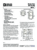
1 A Universal LVDT Signal Conditioner AD698 . FEATURES FUNCTIONAL BLOCK DIAGRAM. Single Chip Solution, Contains Internal Oscillator and Voltage Reference No Adjustments Required VOLTAGE. AMP. Interfaces to Half-Bridge, 4-Wire LVDT REFERENCE. OSCILLATOR. DC Output Proportional to Position 20 Hz to 20 kHz Frequency Range AD698 . B. Unipolar or Bipolar Output Will Also Decode AC Bridge Signals A. B. Outstanding Performance AMP. FILTER. Linearity: A. Output Voltage: 611 V. Gain Drift: 20 ppm/8C (typ). Offset Drift: 5 ppm/8C (typ). PRODUCT DESCRIPTION PRODUCT HIGHLIGHTS.
2 The AD698 is a complete, monolithic Linear Variable Differen- 1. The AD698 offers a single chip solution to LVDT Signal tial Transformer (LVDT) Signal conditioning subsystem. It is conditioning problems. All active circuits are on the mono- used in conjunction with LVDTs to convert transducer mechan - lithic chip with only passive components required to com- ical position to a unipolar or bipolar dc voltage with a high de- plete the conversion from mechanical position to dc voltage. gree of accuracy and repeatability. All circuit functions are 2.
3 The AD698 can be used with many different types of posi- included on the chip. With the addition of a few external passive tion sensors. The circuit is optimized for use with any components to set frequency and gain, the AD698 converts the LVDT, including half-bridge and series opposed, (4 wire). raw LVDT output to a scaled dc Signal . The device will operate configurations. The AD698 accommodates a wide range of with half-bridge LVDTs, LVDTs connected in the series op- input and output voltages and frequencies. posed configuration (4-wire), and RVDTs.
4 3. The 20 Hz to 20 kHz excitation frequency is determined by a The AD698 contains a low distortion sine wave oscillator to single external capacitor. The AD698 provides up to 24 volts drive the LVDT primary. Two synchronous demodulation rms to differentially drive the LVDT primary, and the channels of the AD698 are used to detect primary and second- AD698 meets its specifications with input levels as low as ary amplitude. The part divides the output of the secondary by 100 millivolts rms. the amplitude of the primary and multiplies by a scale factor.
5 This eliminates scale factor errors due to drift in the amplitude 4. Changes in oscillator amplitude with temperature will not af- of the primary drive, improving temperature performance and fect overall circuit performance. The AD698 computes the stability. ratio of the secondary voltage to the primary voltage to deter- mine position and direction. No adjustments are required. The AD698 uses a unique ratiometric architecture to eliminate several of the disadvantages associated with traditional ap- 5. Multiple LVDTs can be driven by a single AD698 either in proaches to LVDT interfacing.
6 The benefits of this new cir- series or parallel as long as power dissipation limits are not cuit are: no adjustments are necessary; temperature stability is exceeded. The excitation output is thermally protected. improved; and transducer interchangeability is improved. 6. The AD698 may be used as a loop integrator in the design of The AD698 is available in two performance grades: simple electromechanical servo loops. Grade Temperature Range Package 7. The sum of the transducer secondary voltages do not need to AD698AP 40 C to +85 C 28-Pin PLCC be constant.
7 AD698SQ 55 C to +125 C 24-Pin Cerdip REV. B. Information furnished by Analog Devices is believed to be accurate and Analog Devices, Inc., 1995. reliable. However, no responsibility is assumed by Analog Devices for its use, nor for any infringements of patents or other rights of third parties which may result from its use. No license is granted by implication or One Technology Way, Box 9106, Norwood. MA 02062-9106, otherwise under any patent or patent rights of Analog Devices. Tel: 617/329-4700 Fax: 617/326-8703. AD698 SPECIFICATIONS (@ T = +258C, V A CM = 0 V, and V+, V = 615 V dc, unless otherwise noted).
8 AD698SQ AD698AP. Parameter Min Typ Max Min Typ Max Unit TRANSFER FUNCTION1 VOUT = A 500 A R2 V. B. OVERALL ERROR TMIN to TMAX % of FS. Signal OUTPUT CHARACTERISTICS. Output Voltage Range 611 611 V. Output Current, TMIN to TMAX 11 11 mA. Short Circuit Current 20 20 mA. Nonlinearity2 TMIN to TMAX 75 6500 75 6500 ppm of FS. Gain Error3 % of FS. Gain Drift 20 6100 20 6100 ppm/ C of FS. Output Offset 61 61 % of FS. Offset Drift 5 625 5 625 ppm/ C of FS. Excitation Voltage Rejection4 100 100 ppm/dB. Power Supply Rejection ( 12 V to 18 V).
9 PSRR Gain 50 300 50 300 ppm/V. PSRR Offset 15 100 15 100 ppm/V. Common-Mode Rejection ( 3 V). CMRR Gain 25 100 25 100 ppm/V. CMRR Offset 2 100 2 100 ppm/V. Output Ripple5 4 4 mV rms EXCITATION OUTPUT CHARACTERISTICS (@ kHz). Excitation Voltage Range 24 24 V rms Excitation Voltage (Resistors Are 1% Absolute Values). (R1 = Open)6 V rms (R1 = k ) V rms (R1 = 487 ) 14 14 V rms Excitation Voltage TC7 100 100 ppm/ C. Output Current 30 50 30 50 mA rms TMIN to TMAX 40 40 mA rms Short Circuit Current 60 60 mA. DC Offset Voltage (Differential, R1 = k ).
10 TMIN to TMAX 30 6100 30 6100 mV. Frequency 20 20 k 20 20 k Hz Frequency TC 200 200 ppm/ C. Total Harmonic Distortion 50 50 dB. Signal INPUT CHARACTERISTICS. A/B Ratio Usable Full-Scale Range Signal Voltage B Channel V rms Signal Voltage A Channel V rms Input Impedance 200 200 k . Input Bias Current (BIN, AIN) 1 5 1 5 A. Signal Reference Bias Current 2 10 2 10 A. Excitation Frequency 0 20 k 0 20 k Hz POWER SUPPLY REQUIREMENTS. Operating Range 13 36 13 36 V. Dual Supply Operation ( 10 V Output) 13 13 V. Single Supply Operation 0 V to +10 V Output V.
