Transcription of AD2S1210 Variable Resolution, 10-bit to 16-Bit RDC ...
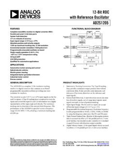
1 Variable resolution , 10-bit to 16-Bit R/D. Converter with Reference Oscillator AD2S1210 . FEATURES FUNCTIONAL BLOCK DIAGRAM. REFERENCE. Complete monolithic resolver-to-digital converter PINS CRYSTAL. 3125 rps maximum tracking rate ( 10-bit resolution ). arc minutes of accuracy REFERENCE VOLTAGE INTERNAL. 10-/12-/14-/ 16-Bit resolution , set by user EXCITATION. OSCILLATOR REFERENCE CLOCK. OUTPUTS. Parallel and serial 10-bit to 16-Bit data ports (DAC) GENERATOR. Absolute position and velocity outputs SYNTHETIC AD2S1210 . System fault detection REFERENCE. Programmable fault detection thresholds Differential inputs ADC. INPUTS TYPE II FAULT FAULT. Incremental encoder emulation FROM TRACKING LOOP DETECTION DETECTION. RESOLVER OUTPUTS. Programmable sinusoidal oscillator on-board ADC. Compatible with DSP and SPI interface standards 5 V supply with V to 5 V logic interface POSITION VELOCITY CONFIGURATION.
2 REGISTER REGISTER DATA I/O. 40 C to +125 C temperature rating REGISTER. EMULATION. ENCODER. ENCODER. APPLICATIONS EMULATION MULTIPLEXER. OUTPUTS. DC and ac servo motor control Encoder emulation DATA BUS OUTPUT. Electric power steering 07467-001. Electric vehicles DATA I/O. RESET. Integrated starter generators/alternators Figure 1. Automotive motion sensing and control GENERAL DESCRIPTION PRODUCT HIGHLIGHTS. The AD2S1210 is a complete 10-bit to 16-Bit resolution tracking 1. Ratiometric tracking conversion. The Type II tracking loop resolver-to-digital converter, integrating an on-board program- provides continuous output position data without mable sinusoidal oscillator that provides sine wave excitation conversion delay. It also provides noise immunity and for resolvers. tolerance of harmonic distortion on the reference and input signals. The converter accepts V p-p 27% input signals, in the range 2.
3 System fault detection. A fault detection circuit can sense of 2 kHz to 20 kHz on the sine and cosine inputs. A Type II. loss of resolver signals, out-of-range input signals, input servo loop is employed to track the inputs and convert the input signal mismatch, or loss of position tracking. The fault sine and cosine information into a digital representation of the detection threshold levels can be individually programmed input angle and velocity. The maximum tracking rate is 3125 rps. by the user for optimization within a particular application. 3. Input signal range. The sine and cosine inputs can accept differential input voltages of V p-p 27%. 4. Programmable excitation frequency. Excitation frequency is easily programmable to a number of standard frequencies between 2 kHz and 20 kHz. 5. Triple format position data. Absolute 10-bit to 16-Bit angular position data is accessed via either a 16-Bit parallel port or a 4-wire serial interface.
4 Incremental encoder emulation is in standard A-quad-B format with direction output available. 6. Digital velocity output. 10-bit to 16-Bit signed digital velocity accessed via either a 16-Bit parallel port or a 4-wire serial interface. Rev. A. Information furnished by analog devices is believed to be accurate and reliable. However, no responsibility is assumed by analog devices for its use, nor for any infringements of patents or other rights of third parties that may result from its use. Specifications subject to change without notice. No One Technology Way, Box 9106, Norwood, MA 02062-9106, license is granted by implication or otherwise under any patent or patent rights of analog devices . Tel: Trademarks and registered trademarks are the property of their respective owners. Fax: 2008 2010 analog devices , Inc. All rights reserved. AD2S1210 . TABLE OF CONTENTS. Features.
5 1 LOS Threshold Register .. 21. Applications .. 1 DOS Overrange Threshold Register .. 21. Functional Block Diagram .. 1 DOS Mismatch Threshold Register .. 21. General Description .. 1 DOS Reset Maximum and Minimum Threshold Registers . 22. Product Highlights .. 1 LOT High Threshold Register .. 22. Revision History .. 2 LOT Low Threshold Register .. 22. 3 Excitation Frequency Register .. 22. Timing Specifications .. 6 Control Register .. 22. Absolute Maximum 8 Software Reset Register .. 23. ESD Caution .. 8 Fault Register .. 23. Pin Configuration and Function Descriptions .. 9 Digital interface .. 24. Typical Performance Characteristics .. 11 SOE Input .. 24. Resolver Format 15 SAMPLE 24. Theory of Operation .. 16 Data Format .. 24. Resolver to Digital Conversion .. 16 Parallel Interface .. 24. Fault Detection Circuit .. 16 Serial Interface .. 28. On-Board Programmable Sinusoidal Oscillator.
6 18 Incremental Encoder Outputs .. 31. Synthetic Reference Generation .. 18 Supply Sequencing and Reset .. 31. Configuration of AD2S1210 .. 20 Circuit Dynamics .. 32. Modes of Operation .. 20 Loop Response Model .. 32. Register 21 Sources of Error .. 33. Position Register .. 21 Outline Dimensions .. 34. Velocity Register .. 21 Ordering Guide .. 34. REVISION HISTORY. 2/10 Rev. 0 to Rev. A. Changes to Typical Performance Characteristics Section .. 11, 12. Changes to Ordering Guide .. 34. 8/08 Revision 0: Initial Version Rev. A | Page 2 of 36. AD2S1210 . SPECIFICATIONS. AVDD = DVDD = V 5%, CLKIN = MHz 25%, EXC, EXC frequency = 10 kHz to 20 kHz ( 10-bit ); 6 kHz to 20 kHz (12-bit);. 3 kHz to 12 kHz (14-bit); 2 kHz to 10 kHz ( 16-Bit ); TA = TMIN to TMAX; unless otherwise noted. 1. Table 1. Parameter Min Typ Max Unit Conditions/Comments SINE, COSINE INPUTS 2. Voltage Amplitude V p-p Sinusoidal waveforms, differential SIN to SINLO, COS to COSLO.
7 Input Bias Current A VIN = V p-p, CLKIN = MHz Input Impedance 485 k VIN = V p-p, CLKIN = MHz Phase Lock Range 44 +44 Degrees Sine/cosine vs. EXC output, Control Register D3 = 0. Common-Mode Rejection 20 arc sec/V 10 Hz to 1 MHz, Control Register D4 = 0. ANGULAR ACCURACY 3. Angular Accuracy + 1 LSB 5 + 1 LSB arc min B, D grades 5 + 1 LSB 10 + 1 LSB arc min A, C grades resolution 10, 12, 14, 16 Bits No missing codes Linearity INL. 10-bit 1 LSB B, D grades 2 LSB A, C grades 12-bit 2 LSB B, D grades 4 LSB A, C grades 14-bit 4 LSB B, D grades 8 LSB A, C grades 16-Bit 16 LSB B, D grades 32 LSB A, C grades Linearity DNL LSB. Repeatability 1 LSB. VELOCITY OUTPUT. Velocity Accuracy 4. 10-bit 2 LSB B, D grades, zero acceleration 4 LSB A, C grades, zero acceleration 12-bit 2 LSB B, D grades, zero acceleration 4 LSB A, C grades, zero acceleration 14-bit 4 LSB B, D grades, zero acceleration 8 LSB A, C grades, zero acceleration 16-Bit 16 LSB B, D grades, zero acceleration 32 LSB A, C grades, zero acceleration resolution 5 9, 11, 13, 15 Bits DYNAMNIC PERFORMANCE.
8 Bandwidth 10-bit 2000 6500 Hz 2900 5300 Hz CLKIN = MHz 12-bit 900 2800 Hz 1200 2200 Hz CLKIN = MHz 14-bit 400 1500 Hz 600 1200 Hz CLKIN = MHz 16-Bit 100 350 Hz 125 275 Hz CLKIN = MHz Rev. A | Page 3 of 36. AD2S1210 . Parameter Min Typ Max Unit Conditions/Comments Tracking Rate 10-bit 3125 rps CLKIN = MHz 2500 CLKIN = MHz 12-bit 1250 rps CLKIN = MHz 1000 CLKIN = MHz 14-bit 625 rps CLKIN = MHz 500 CLKIN = MHz 16-Bit rps CLKIN = MHz 125 CLKIN = MHz Acceleration Error 10-bit 30 arc min At 50,000 rps2, CLKIN = MHz 12-bit 30 arc min At 10,000 rps2, CLKIN = MHz 14-bit 30 arc min At 2500 rps2, CLKIN = MHz 16-Bit 30 arc min At 125 rps2, CLKIN = MHz Settling Time 10 Step Input 10-bit ms To settle to within 2 LSB , CLKIN = MHz 12-bit ms To settle to within 2 LSB, CLKIN = MHz 14-bit ms To settle to within 2 LSB , CLKIN = MHz 16-Bit 40 ms To settle to within 2 LSB, CLKIN = MHz Settling Time 179 Step Input 10-bit ms To settle to within 2 LSB , CLKIN = MHz 12-bit ms To settle to within 2 LSB, CLKIN = MHz 14-bit ms To settle to within 2 LSB , CLKIN = MHz 16-Bit 45 66 ms To settle to within 2 LSB.
9 CLKIN = MHz EXC, EXC OUTPUTS. Voltage V p-p Load 100 A, typical differential output (EXC to EXC) = V p-p Center Voltage V. Frequency 2 20 kHz EXC/EXC DC Mismatch 30 mV. EXC/EXC AC Mismatch 100 mV. THD 58 dB First five harmonics VOLTAGE REFERENCE. REFOUT V IOUT = 100 A. Drift 100 ppm/ C. PSRR 60 dB. CLKIN, XTALOUT 6. VIL Voltage Input Low V. VIH Voltage Input High V. LOGIC INPUTS. VIL Voltage Input Low V VDRIVE = V to V. V VDRIVE = V to V. VIH Voltage Input High V VDRIVE = V to V. V VDRIVE = V to V. IIL Low Level Input Current (Non 10 A. Pull-Up). IIL Low Level Input Current (Pull-Up) 80 A RES0, RES1, RD, WR/FSYNC, A0, A1, and RESET pins IIH High Level Input Current 10 A. LOGIC OUTPUTS. VOL Voltage Output Low V VDRIVE = V to V. VOH Voltage Output High V VDRIVE = V to V. V VDRIVE = V to V. IOZH High Level Three-State Leakage 10 A. IOZL Low Level Three-State Leakage 10 A. Rev.
10 A | Page 4 of 36. AD2S1210 . Parameter Min Typ Max Unit Conditions/Comments POWER REQUIREMENTS. AVDD V. DVDD V. VDRIVE V. POWER SUPPLY. IAVDD 12 mA. IDVDD 35 mA. IOVDD 2 mA. 1. Temperature ranges are as follows: A, B grades: 40 C to +85 C; C, D grades: 40 C to +125 C. 2. The voltages, SIN, SINLO, COS, and COSLO, relative to AGND, must always be between V and AVDD V. 3. All specifications within the angular accuracy parameter are tested at constant velocity, that is, zero acceleration. 4. The velocity accuracy specification includes velocity offset and dynamic ripple. 5. For example when RES0 = 0 and RES1 = 1, the position output has a resolution of 12 bits. The velocity output has a resolution of 11 bits with the MSB indicating the direction of rotation. In this example, with a CLKIN frequency of MHz the velocity LSB is rps, that is, 1000 rps/(211). 6. The clock frequency of the AD2S1210 can be supplied with a crystal, an oscillator, or directly from a DSP/microprocessor digital output.