Transcription of AD8476 Fully Differential Unity Gain Amplifier and ADC ...
1 Low Power, Unity Gain, Fully Differential Amplifier and adc driver data Sheet AD8476 Rev. B Information furnished by analog devices is believed to be accurate and reliable. However, no responsibility is assumed by analog devices for its use, nor for any infringements of patents or other rights of third parties that may result from its use. Specifications subject to change without notice. No license is granted by implication or otherwise under any patent or patent rights of analog devices . Trademarks and registered trademarks are the property of their respective owners. One Technology Way, Box 9106, Norwood, MA 02062-9106, Tel: Fax: 2011 2012 analog devices , Inc. All rights reserved. FEATURES Very low power 330 A supply current Extremely low harmonic distortion 126 HD2 at 10 kHz 128 HD3 at 10 kHz Fully Differential or single-ended inputs/outputs Differential output designed to drive precision ADCs Drives switched capacitor and - ADCs Rail-to-rail outputs VOCM pin adjusts output common mode Robust overvoltage up to 18 V beyond supplies High performance Suitable for driving 16-bit converter up to 250 kSPS 39 nV/ Hz output noise 1 ppm/ C gain drift maximum 200 V maximum output offset 10 V/ s slew rate 6 MHz bandwidth Single supply: 3 V to 18 V Dual supplies.
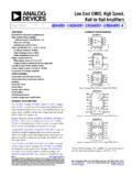
2 V to 9 V APPLICATIONS ADC driver Differential instrumentation Amplifier building block Single-ended-to- Differential converter Battery-powered instruments FUNCTIONAL BLOCK DIAGRAM 10k 10k 10k 10k INN1+VS2 VOCM3+OUT4 INP8 VS7NC6 = NO NOT CONNECT TO THIS Figure 1. 8-Lead MSOP 121110134NC OUT+OUT9 VOCMINPINN2 INPINN6+VS5+VS7+VS8+VS16 VS15 VS14 VS13 VS10k 10k 10k 10k = NO CONNECT. DO NOT CONNECTTO THIS Figure 2. 16-Lead LFCSP GENERAL DESCRIPTION The AD8476 is a very low power, Fully Differential precision Amplifier with integrated gain resistors for Unity gain. It is an ideal choice for driving low power, high performance ADCs as a single-ended-to- Differential or Differential -to- Differential Amplifier . It provides a precision gain of 1, common-mode level shifting, low temperature drift, and rail-to-rail outputs for maximum dynamic range.
3 The AD8476 also provides overvoltage protection from large industrial input voltages up to 23 V while operating on a dual 5 V supply. Power dissipation on a single 5 V supply is only m W. The AD8476 works well with SAR, - , and pipeline converters. The high current output stage of the part allows it to drive the switched capacitor front-end circuits of many ADCs with minimal error. Unlike many Differential drivers on the market, the AD8476 is a high precision Amplifier . With 200 V maximum output offset, 39 nV/ Hz noise, and 102 dB THD + N at 10 kHz, the AD8476 pairs well with low power, high accuracy converters. Considering its low power consumption and high precision, the slew-enhanced AD8476 has excellent speed, settling to 16- bit precision for 250 kSPS acquisition times. The AD8476 is available in space-saving 16-lead, 3 mm 3 mm LFCSP and 8-lead MSOP packages.
4 It is Fully specified over the 40 C to +125 C temperature range. AD8476 data Sheet Rev. B | Page 2 of 24 TABLE OF CONTENTS Features .. 1 Applications .. 1 Functional Block Diagram .. 1 General Description .. 1 Revision History .. 2 Specifications .. 3 Absolute Maximum Ratings .. 5 Thermal Resistance .. 5 Maximum Power Dissipation .. 5 ESD Caution .. 5 Pin Configuration and Function Descriptions .. 6 Typical Performance Characteristics .. 8 Terminology .. 16 Theory of Operation .. 17 Overview .. 17 Circuit Information .. 17 DC Precision .. 17 Input Voltage Range .. 18 Driving the 18 Power Supplies .. 18 Applications Information .. 19 Typical Configuration .. 19 Single-Ended-to- Differential Conversion .. 19 Setting the Output Common-Mode Voltage .. 19 Low Power ADC Driving .. 20 Outline Dimensions.
5 21 Ordering Guide .. 22 REVISION HISTORY 5/12 Rev. A to Rev. B Added LFCSP Throughout .. 1 Added Harmonic Distortion Values to Features Section and Changed Bandwidth from 5 MHz to 6 MHz .. 1 Changed 3 dB Small Signal Bandwidth from 5 MHz to 6 MHz, Changed HD2 from 120 dB to 126 dB, and Changed HD3 from 122 dB to 128 dB, Table 1 .. 3 Changes to Figure 17 and Figure 19 .. 10 Changes to Figure 25 .. 11 Changes to Figure 30 .. 12 Added Low Power ADC Driving Section .. 20 Updated Outline Dimensions .. 21 Changes to Ordering Guide .. 22 11/11 Rev. 0 to Rev. A Changes to Table 1 .. 3 Changes to Typical Performance Characteristics .. 7 Added Figure 39; Renumbered Sequentially .. 13 Added Table 5 .. 18 Removed Low Power ADC Driving Section .. 19 Removed Figure 52 .. 19 10/11 Revision 0: Initial Version data Sheet AD8476 Rev.
6 B | Page 3 of 24 SPECIFICATIONS VS = +5 to 5 V, VOCM = midsupply, VOUT = V+OUT V OUT, RL = 2 k Differential , referred to output (RTO), TA = 25 C, unless otherwise noted. Table 1 . Parameter Test Conditions/Comments B Grade A Grade Unit Min Typ Max Min Typ Max DYNAMIC PERFORMANCE 3 dB Small Signal Bandwidth VOUT = 200 mV p-p 6 6 MHz 3 dB Large Signal Bandwidth VOUT = 2 V p-p 1 1 MHz Slew Rate VOUT = 2 V step 10 10 V/ s Settling Time to VOUT = 2 V step s Settling Time to VOUT = 2 V step s NOISE/DISTORTION1 THD + N f = 10 kHz, VOUT = 2 V p-p, 22 kHz filter 102 102 dB HD2 f = 10 kHz, VOUT = 2 V p-p 126 126 dB HD3 f = 10 kHz, VOUT = 2 V p-p 128 128 dB IMD3 f1 = 95 kHz, f2 = 105 kHz, VOUT = 2 V p-p 82 82 dBc Output Voltage Noise f = Hz to 10 Hz 6 6 V p-p Spectral Noise Density f = 10 kHz 39 39 nV/ Hz GAIN 1 1 V/V Gain Error RL = % Gain Drift 40 C TA +125 C 1 1 ppm/ C Gain Nonlinearity VOUT = 4 V p-p 5 5 ppm OFFSET AND CMRR Differential Offset2 50 200 50 500 V vs.
7 Temperature 40 C TA +125 C 900 900 V Average TC 40 C TA +125 C 1 4 1 4 V/ C vs. Power Supply (PSRR) VS = V to 9 V 90 90 dB Common-Mode Offset2 50 50 V Common-Mode Rejection Ratio VIN,cm = 5 V 90 80 dB INPUT CHARACTERISTICS Input Voltage Range3 Differential input VS + +VS VS + +VS V Single-ended input 2( VS + ) 2(+V ) 2( VS + ) 2(+VS ) V Impedance4 Vcm = VS/2 Single-Ended Input k Differential Input 20 20 k Common-Mode Input 10 10 k OUTPUT CHARACTERISTICS Output Swing VS = +5 V VS + +VS VS + +VS VS = 5 V VS + +VS VS + +VS Output Balance Error VOUT,cm/ VOUT,dm 90 80 dB Output Impedance Capacitive Load Per output 20 20 pF Short-Circuit Current Limit 35 35 mA VOCM CHARACTERISTICS VOCM Input Voltage Range VS + 1 +VS 1 VS + 1 +VS 1 V VOCM Input Impedance 500 500 k VOCM Gain Error % AD8476 data Sheet Rev.
8 B | Page 4 of 24 Parameter Test Conditions/Comments B Grade A Grade Unit Min Typ Max Min Typ Max POWER SUPPLY Specified Supply Voltage 5 5 V Operating Supply Voltage Range 3 18 3 18 V Supply Current VS = +5 V, TA = 25 C 300 330 300 330 A VS = 5 V, TA = 25 C 330 380 330 380 A Over Temperature 40 C TA +125 C 400 500 400 500 A TEMPERATURE RANGE Specified Performance Range 40 +125 40 +125 C 1 Includes Amplifier voltage and current noise, as well as noise of internal resistors. 2 Includes input bias and offset current errors. 3 The input voltage range is a function of the voltage supplies and ESD diodes. 4 Internal resistors are trimmed to be ratio matched but have 20% absolute accuracy. data Sheet AD8476 Rev. B | Page 5 of 24 ABSOLUTE MAXIMUM RATINGS Table 2.
9 Parameter Rating Supply Voltage 10 V Maximum Voltage at Any Input Pin +VS + 18 V Minimum Voltage at Any Input Pin VS 18 V Storage Temperature Range 65 C to +150 C Specified Temperature Range 40 C to +125 C Package Glass Transition Temperature (TG) 150 C ESD (Human Body Model) 2500 V Stresses above those listed under Absolute Maximum Ratings may cause permanent damage to the device. This is a stress rating only; functional operation of the device at these or any other conditions above those indicated in the operational section of this specification is not implied. Exposure to absolute maximum rating conditions for extended periods may affect device reliability. THERMAL RESISTANCE The JA values in Ta b l e 3 assume a 4-layer JEDEC standard board with zero airflow. Table 3. Thermal Resistance Package Type JA Unit 8-Lead MSOP C/W 16-Lead LFCSP, 3 mm 3 mm C/W MAXIMUM POWER DISSIPATION The maximum safe power dissipation for the AD8476 is limited by the associated rise in junction temperature (TJ) on the die.
10 At approximately 150 C, which is the glass transition temperature, the properties of the plastic change. Even temporarily exceeding this temperature limit may change the stresses that the package exerts on the die, permanently shifting the parametric performance of the amplifiers. Exceeding a temperature of 150 C for an extended period may result in a loss of functionality. ESD CAUTION AD8476 data Sheet Rev. B | Page 6 of 24 PIN CONFIGURATION AND FUNCTION DESCRIPTIONS INN1+VS2 VOCM3+OUT4 INP8 VS7NC6 OUT5AD8476 TOP VIEW(Not to Scale)10195-004 NOTES1. PINS LABELED NC CAN BE ALLOWEDTO FLOAT, BUT IT IS BETTER TO CONNECTTHESE PINS TO GROUND. AVOID ROUTINGHIGH SPEED SIGNALS THROUGH THESEPINS BECAUSE NOISE COUPLING MAY RESULT. Figure 3. 8-Lead MSOP Pin Configuration Table 4. 8-Lead MSOP Pin Function Descriptions Pin No.
