Transcription of Analog CMOS/VLSI Design - USF
1 USF: Analog cmos vlsi Design . Spring 2014 1 Catalog Description: Design of Analog circuits for CMOS/VLSI Design . Op-amps, comparators, D to A and A to D converters. Switched capacitor filters. Analog simulation. PR: EEL 4301 (Electronics II) or EEL 4705 (Logic Design ) or CI. Textbook: Design of Analog cmos Integrated Circuits, by B. Razavi. ISBN 0-07-238032-2 McGraw-Hill Publishers, 2001. References: The material will be supplemented from other sources as well Instructor: Dr. V. K. Jain, Distinguished Professor Office: ENB 372 Phone: (813) 974-4741 Goals: To familiarize the student with the principles and Design approaches for Analog cmos vlsi circuits, and their applications. Simulations through ADS and/or PSPICE are included. Typical application areas: wireless communications, biomedical systems, digital ( cmos ) cameras, sensors including bio-sensors, power systems and power grid, and ultralow power signal processing.
2 Prerequisites by Topic: Electronic circuit analysis Topics will be selected from: 1. cmos Device Physics; cmos process, device geometry and models 2. Single stage amplifiers: common source, source follower, common-gate 3. Differential amplifiers 4. Passive and active current mirrors 5. Frequency response of amplifiers; feedback; stability and frequency compensation 6. Switched capacitor circuits 7. Oscillators and phase-locked loops 8. Analog -to-digital and digital-to- Analog converters 9. Mixed signal circuits 10. cmos processing technology: photolithography, oxidation, ion implantation, deposition and etching, interconnects 11. Circuit model extraction from physical layouts, and their simulation 12. Applications: communications, sensing, bio-medical, power grid, digital cameras, | Time A/D conversion, System on a chip and 3D stacking | permitting Grading: Midterm exam or Term paper (class decision) 40 Simulation assignments 10 Final exam 50 100 Slightly different quizzes/exams may be given for 6000, 5000, and 4000 level sections.
3 The date for the exam will be announced a week before the event. Missed Exams: All exams, as scheduled, are mandatory. There will be no makeup exams. A missed exam will automatically lead to a zero score on that exam/quiz. Guidelines for the term paper, if applicable, will be posted in the appropriate week.. Continued on the next page (G and UG; also on-line) Analog CMOS/VLSI Design Spring Semester 2014 USF: Analog cmos vlsi Design . Spring 2014 2 Consultation hours: Mondays: 2 pm to 3 pm; Tuesdays: 4 pm to 5 pm; Fridays: 1 pm to 2 pm. Venue: ENB 372 (office) or ENB 349 (Lab) Questions Regarding Exams and Grading: All questions relating to exams and grading policy must be raised only in the class (not in the consultation hours or through emails and phone calls, in order to be fair to all). On the other hand, discussion on an individual s graded exam, if any, will be carried out on a one-on-one basis, not during the class.
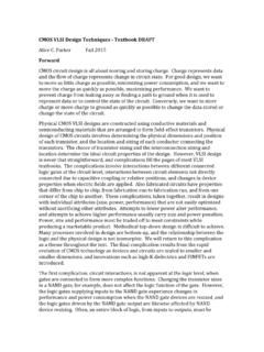
4 Homework: The homework policy will be announced in the class. Class attendance: Although not mandatory, class attendance is highly encouraged. email: If the term paper option is chosen by the class, it may be emailed (before the yet to be announced deadline) to Academic continuity in the event of campus closure due to an emergency: In the event of a campus closure due to an emergency, we fully intend to continue delivery of instruction using an alternative ( , electronic) mode. Further information will be provided if and when necessary. Figure: Just a few examples that are candidates for discussion in the course (although they may not be easily understandable at the beginning of the semester) Distribution policy: It is recommended that the class materials not be distributed (or sold) to anyone outside this class. Academic Integrity for All Electrical Engineering Courses: Please see and comply with the companion document on Academic Integrity (Fall 2013 version).
5 Charge-pump based PLLVinQAQBR esetDCKDCKQQVDDRPCPVoutVCOS1S2I1I2 Charge-pump based PLLVinQAQBR esetDCKDCKQQVDDRPCPVoutVCOS1S2I1I2 VinQAQBR esetDCKDCKQQVDDRPCPVoutVCOS1S2I1I2An Example Application of Current ITXYPAn Example Application of Current ITXYP2 mpolyp-welln +n +p-substratep+pp-welln+n+Photo diodeReset TransistorTransfer 10 mTGYR esetVDDAPS FabricationCharge-pump based PLLVinQAQBR esetDCKDCKQQVDDRPCPVoutVCOS1S2I1I2 Charge-pump based PLLVinQAQBR esetDCKDCKQQVDDRPCPVoutVCOS1S2I1I2 VinQAQBR esetDCKDCKQQVDDRPCPVoutVCOS1S2I1I2An Example Application of Current ITXYPAn Example Application of Current ITXYP2 mpolyp-welln +n +p-substratep+pp-welln+n+Photo diodeReset TransistorTransfer 10 mTGYR esetVDDAPS Fabricatio