Example: barber
ATMEGA16U2 - Arduino
Card Interface) SSC (Synchronous Serial Controller) A11 A13 A22 D1 D3 D5 D7 D14 D12 NWR1/NBS1 NANDCLE NANDOE External Memory BUS SMC (Static Memory Controller) NFC (NAND Flash PA14 PD0 PD2 PD6 PA7 ... JTAG 1 +3V3 2 JTAG_TMS/SWDIO 3 GND 4 JTAG_TCK/SWCLK 5 GND 6 JTAG_TDO/TRACESWO 7 8 JTAG_TDI JTAG_RESET 9 GND …
Tags:
Information
Domain:
Source:
Link to this page:
Documents from same domain

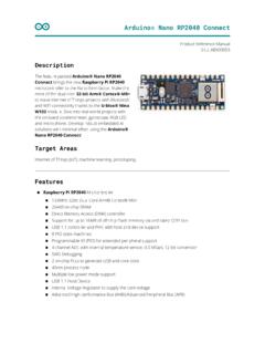
Arduino Portenta H7
content.arduino.cc8-bit camera interface (up to 80 MHz) 11 analog peripherals 3× ADCs with 16-bit max. resolution (up to 36 channels, up to 3.6 MSPS) 1× temperature sensor 2× 12-bit D/A converters (1 MHz) 2× ultra-low-power comparators 2× operational amplifiers (7.3 MHz bandwidth)
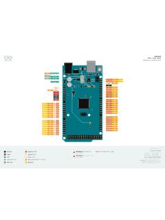
PB7 LED BUILTIN ATMEGA16U2
content.arduino.ccD21/SCL VIN 6-20 V input to the board. MAXIMUM current per +3.3V pin is 50mA MAXIMUM current per I/O pin is 20mA. Analog Communication Timer Interrupt ... D23 D25 D27 D29 D31 D33 D35 D37 D39 D41 D43 ~D45 D47 D49 D51 D53 GND PA0 PA2 PA4 PA6 PC7 PC5 PC3 PC1 PD7 PG1 PL7 PL5 PL3 PL1 PB3 PB1 AD0 AD2 AD4 AD6 A15 A13 A11 A9 RD CIPO SPI SCK …

MEGA2560 Rev3e - Arduino
content.arduino.ccr e f e r e n c e u d e s i g n s a r e p r o v i d e d " a s i s " a n d " w i t h u a l l t f a u l t s. r a r d u i n o s a d i s c l a i m s a l l o t h e r a w a ...

MAXIMUM current per I/O
content.arduino.ccMAXIMUM current per +3.3V pin is 50mA MAXIMUM current per I/O pin is 20mA NOTE: CIPO/COPI have previously been referred to as MISO/MOSI. Analog Communication Timer Interrupt Sercom Internal Pin I V Ground Power LED SWD Pin Digital Pin Analog Pin Other Pin Microcontroller’s Port Default ast update: 3/0/202 D12 ~D11 ~D10 ~D9 D8 D7 ~D6 ~D5 D4 ...
Description - Arduino
content.arduino.cc3 Functional overview 3.1 Block Diagram 3.2 Board Topology 3.3 Processor 3.4 WiFi/Bluetooth connectivity 3.5 6-axis IMU 3.6 External memory 3.7 Cryptography 3.8 Microphone 3.9 RGB LED 3.10 Power Tree 4 Board Operation 4.1 Getting started - IDE 4.2 Getting started - Arduino Web Editor 4.3 Getting started - Arduino IoT Cloud 4.4 Sample Sketches 4 ...

ATmega328P - Arduino
content.arduino.ccATmega328P [DATASHEET] 7810D–AVR–01/15 2 I/O and packages 23 programmable I/O lines 32-lead TQFP, and 32-pad QFN/MLF Operating voltage: 2.7V to 5.5V for ATmega328P

PB5 D13 D12 PB4 CIPO PB3 COPI PB2 A0 D14 ~D9 PB1 ... - …
content.arduino.ccT C C ASA . I . T //. ///./ C C O M CA USA. Ground Power LED I VIN Default ast update: 30/0/2021 STORE.ARDUINO.CC/NANO 7-12 V input to the board.

NanoV3.3 - Arduino
content.arduino.ccTitle: NanoV3.3.sch Created Date: 1/23/2019 2:50:23 PM

Arduino(TM) UNO Rev3
content.arduino.ccr e f e r e n c e u d e s i g n s a r e p r o v i d e d " a s i s " a n d " w i t h u a l l t f a u l t s. r a r d u i n o s a d i s c l a i m s a l l o t h e r a w a ...
Related documents
ATmega16A - Microchip Technology
ww1.microchip.comIf the JTAG interface is enabled, the pull-up resistors on pins PC5(TDI), PC3(TMS) and PC2(TCK) will be activated even if a reset occurs. Port C also serves the functions of the JTAG interface an d other special features of the ATmega16A as listed on page 59. 2.2.6 Port D …
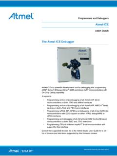
The Atmel-ICE Debugger - Microchip Technology
ww1.microchip.commicrocontrollers on both JTAG and aWire interfaces • Programming and on-chip debugging of all Atmel AVR XMEGA® family devices on both JTAG and PDI 2-wire interfaces • Programming (JTAG, SPI, UPDI) and debugging of all Atmel AVR 8-bit microcontrollers with OCD support on either JTAG, debugWIRE or UPDI interfaces

Training JTAG Interface - Lauterbach
www2.lauterbach.com©1989-2021 Lau terbach GmbH Training JTAG Interface | 6 JTAG Basics JTAG is the name used for the IEEE 1149.1 standard entitled Standard Test Access Port and Boundary- Scan Architecture for test access ports (TAP) used for testing printed circuit boards (PCB) using boundary scan. JTAG is the acronym for Joint Test Action Group, the name of the group of …

UM1075 User manual - STMicroelectronics
www.st.com• JTAG/serial wire debugging (SWD) specific features – 1.65 V to 3.6 V application voltage suppo rted on the JTAG/SWD interface and 5 V tolerant inputs – JTAG cable for connection to a standard JTAG 20-pin pitch 2.54 mm connector – Supports JTAG communication – Supports serial wire debug (SWD) and serial wire viewer (SWV) communication

AN0062: Programming Internal Flash Over the Serial Wire ...
www.silabs.com1 Debug Interface Overview 1.1 Serial Wire Debug Serial Wire Debug (SWD) is a two-wire protocol for accessing the ARM debug interface. It is part of the ARM Debug Interface Specification v5 and is an alternative to JTAG. The physical layer of SWD consists of two lines: • SWDIO: a bidirectional data line • SWCLK: a clock driven by the host
Platform Cable USB II - Xilinx
www.xilinx.comInterface (SPI) flash memory devices Note: Direct SPI flash memory programming supported in Xilinx iMPACT software v10.1. † Indirectly programs selected SPI or parallel flash memory devices via FPGA JTAG port † Highly optimized for use with Xilinx design tools † Vivado® design tools or ISE® design tools † Embedded Development Kit
PM0075 Programming manual - STMicroelectronics
www.st.commicrocontroller using the JTAG protocol, the SWD protocol or the boot loader while the device is mounted on the user application board. I-Code: this bus connects the Instruction bus of the Cortex-M3 core to the Flash instruction interface. Prefetch is performed on this bus.

Platform Flash In-System Programmable Configuration …
www.xilinx.comJTAG Interface Memory OSC Serial or Parallel Decompressor DS123_19_031908. Platform Flash In-System Programmable Configuration PROMs DS123 (v2.19) June 6, 2016 www.xilinx.com Product Specification 3 R See UG161, Platform Flash PROM User Guide, for detailed guidelines on PROM-to-FPGA configuration hardware

RISC-V External Debug Support Version 0.13.2 ...
riscv.orgRISC-V External Debug Support Version 0.13.2 d5029366d59e8563c08b6b9435f82573b603e48e Editors: Tim Newsome <tim@si ve.com>, SiFive, Inc. Megan Wachs <megan@si ve.com ...