Transcription of Platform Flash In-System Programmable Configuration …
1 DS123 ( ) June 6, Specification1 Copyright 2003 2016 xilinx , Inc. xilinx , the xilinx logo, Artix, ISE, Kintex, Spartan, Virtex, Vivado, Zynq, and other designated brands included herein are trademarks of xilinx in the United States and other countries. All other trademarks are the property of their respective In-System Programmable PROMs for Configuration of xilinx FPGAs Low-Power Advanced CMOS NOR Flash Process Endurance of 20,000 Program/Erase Cycles Operation over Full Industrial Temperature Range ( 40 C to +85 C) IEEE Standard Boundary-Scan ( jtag ) Support for Programming, Prototyping, and Testing jtag Command Initiation of Standard FPGA Configuration Cascadable for Storing Longer or Multiple Bitstreams Dedicated Boundary-Scan ( jtag ) I/O Power Supply (VCCJ)
2 I/O Pins Compatible with Voltage Levels Ranging From to Design Support Using the xilinx ISE Alliance and Foundation Software Packages XCF01S/XCF02S/XCF04S Supply Voltage Serial FPGA Configuration interface Available in Small-Footprint VO20 and VOG20 Packages XCF08P/XCF16P/XCF32P Supply Voltage Serial or Parallel FPGA Configuration interface Available in Small-Footprint VOG48, FS48, and FSG48 Packages Design Revision Technology Enables Storing and Accessing Multiple Design Revisions for Configuration Built-In Data Decompressor Compatible with xilinx Advanced Compression TechnologyDescriptionXilinx introduces the Platform Flash series of In-System Programmable Configuration PROMs.
3 Available in 1 to 32 Mb densities, these PROMs provide an easy-to-use, cost-effective, and reprogrammable method for storing large xilinx FPGA Configuration bitstreams. The Platform Flash PROM series includes both the XCFxxS PROM and the XCFxxP PROM. The XCFxxS version includes 4 Mb, 2 Mb, and 1 Mb PROMs that support Master Serial and Slave Serial FPGA Configuration modes (Figure 1, page 2). The XCFxxP version includes 32 Mb, 16 Mb, and 8 Mb PROMs that support Master Serial, Slave Serial, Master SelectMAP, and Slave SelectMAP FPGA Configuration modes (Figure 2, page 2).
4 When driven from a stable, external clock, the PROMs can output data at rates up to 33 MHz. Refer to "AC Electrical Characteristics," page 16 for timing summary of the Platform Flash PROM family members and supported features is shown in Table Flash In-System ProgrammableConfiguration PROMsDS123 ( ) June 6, 2016 Product SpecificationRTable 1: Platform Flash PROM FeaturesDeviceDensity(Mb)VCCINT(V)VCCO Range(V)VCCJ Range(V)PackagesProgram In-System via JTAGS erial (1) Notes: supports storage of a design revision only when cascaded with another XCFxxP PROM.
5 See "Design Revisioning," page 8 for Flash In-System Programmable Configuration PROMsDS123 ( ) June 6, Specification2 RWhen the FPGA is in Master Serial mode, it generates a Configuration clock that drives the PROM. With CF High, a short access time after CE and OE are enabled, data is available on the PROM DATA (D0) pin that is connected to the FPGA DIN pin. New data is available a short access time after each rising clock edge. The FPGA generates the appropriate number of clock pulses to complete the the FPGA is in Slave Serial mode, the PROM and the FPGA are both clocked by an external clock source, or optionally, for the XCFxxP PROM only, the PROM can be used to drive the FPGA s Configuration XCFxxP version of the Platform Flash PROM also supports Master SelectMAP and Slave SelectMAP (or Slave Parallel) FPGA Configuration modes.
6 When the FPGA is in Master SelectMAP mode, the FPGA generates a Configuration clock that drives the PROM. When the FPGA is in Slave SelectMAP Mode, either an external oscillator generates the Configuration clock that drives the PROM and the FPGA, or optionally, the XCFxxP PROM can be used to drive the FPGA s Configuration clock. With BUSY Low and CF High, after CE and OE are enabled, data is available on the PROMs DATA (D0-D7) pins. New data is available a short access time after each rising clock edge. The data is clocked into the FPGA on the following rising edge of the CCLK.
7 A free-running oscillator can be used in the Slave Parallel/Slave SelectMAP XCFxxP version of the Platform Flash PROM provides additional advanced features. A built-in data decompressor supports utilizing compressed PROM files, and design revisioning allows multiple design revisions to be stored on a single PROM or stored across several PROMs. For design revisioning, external pins or internal control bits are used to select the active design Platform Flash PROM devices can be cascaded to support the larger Configuration files required when targeting larger FPGA devices or targeting multiple FPGAs daisy chained together.
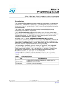
8 When utilizing the advanced features for the XCFxxP Platform Flash PROM, such as design revisioning, programming files which span cascaded PROM devices can only be created for cascaded chains containing only XCFxxP PROMs. If the advanced XCFxxP features are not enabled, then the cascaded chain can include both XCFxxP and XCFxxS Target - Figure 1 Figure 1:XCFxxS Platform Flash PROM Block DiagramX-Ref Target - Figure 2 FIFigure 2:XCFxxP Platform Flash PROM Block DiagramControlandJTAGI nterfaceMemorySerialInterfaceDATA (D0)Serial ModeDataAddressCLKCETCKTMSTDITDOOE/RESET CEOD atads123_01_30603 CFCLKOUTCEODATA (D0)(Serial/Parallel Mode)D[1:7](Parallel Mode)TCKTMSTDITDOCLKCEEN_EXT_SELOE/RESET BUSYDataDataAddressREV_SEL [1.]
9 0]CFControlandJTAGI nterfaceMemoryOSCS erialor ParallelInterfaceDecompressorDS123_19_03 1908 Platform Flash In-System Programmable Configuration PROMsDS123 ( ) June 6, Specification3 RSee UG161, Platform Flash PROM User Guide, for detailed guidelines on PROM-to-FPGA Configuration hardware connections, for software usage, for a reference list of xilinx FPGAs, and for the respective compatible Platform Flash PROMs. Table 2 lists the Platform Flash PROMs and their Platform Flash PROM is a reprogrammable NOR Flash device (refer "Quality and Reliability Characteristics," page 14 for the program/erase specifications).
10 Reprogramming requires an erase followed by a program operation. A verify operation is recommended after the program operation to validate the correct transfer of data from the programmer source to the Platform Flash programming solutions are ProgrammingIn-System Programmable PROMs can be programmed individually, or two or more can be daisy-chained together and programmed In-System via the standard 4-pin jtag protocol as shown in Figure 3. In-System programming offers quick and efficient design iterations and eliminates unnecessary package handling or socketing of devices.