Transcription of Bidirectional, Zero Drift, Current Sense Amplifier Data ...
1 bidirectional , zero drift , Current Sense Amplifier data sheet AD8417 Rev. E Document Feedback Information furnished by analog devices is believed to be accurate and reliable. However, no responsibi lity is assumed by analog devices for its use, nor for any infringements of patents or other rights of third parties that may result from its use. Specifications subject to change without notice. No license is granted by implication or otherwise under any patent or patent rights of analog devices . Trademarks and registered trademarks are the property of their respective owners. One Technology Way, Box 9106, Norwood, MA 02062-9106, Tel: 2013 2020 analog devices , Inc.
2 All rights reserved. Technical Support FEATURES Typical V/ C offset drift Maximum 400 V voltage offset over full temperature range V to V power supply operating range EMI filters included High common-mode input voltage range 2 V to +70 V continuous 3 V to +80 V survival Initial gain = 60 V/V Wide operating temperature range AD8417WB (8-lead MSOP, 8-lead SOIC_N, and 10-lead MSOP) and AD8417B (8-lead MSOP): 40 C to +125 C AD8417WH (8-lead SOIC_N and 8-lead MSOP): 40 C to +150 C bidirectional operation Available in 8-lead SOIC_N, 8-lead MSOP, and FMEA tolerant 10-lead MSOP pinout CMRR: 86 dB, dc to 10 kHz AEC-Q100 qualified for automotive applications APPLICATIONS High-side Current sensing in Motor controls Solenoid controls Power management Low-side Current sensing Diagnostic protection GENERAL DESCRIPTION The AD8417 is a high voltage, high resolution Current Sense Amplifier .
3 It features an initial gain of 60 V/V, with a maximum gain error over the entire temperature range. The buffered output voltage directly interfaces with any typical converter. The AD8417 offers excellent input common-mode rejection from 2 V to +70 V. The AD8417 performs bidirectional Current measurements across a shunt resistor in a variety of automotive and industrial applications, including motor control, power management, and solenoid control. The AD8417 offers breakthrough performance throughout the 40 C to +150 C temperature range (AD8417WH). It features a zero drift core, which leads to a typical offset drift of V/ C throughout the operating temperature range and the common-mode voltage range.
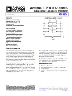
4 The AD8417 is qualified for automotive applications. The device includes electromagnetic interference (EMI) filters and patented ( Patent 8,624,668 B2) circuitry to enable output accuracy with pulse-width modulation (PWM) type input common-mode voltages. The typical input offset voltage is 200 V. The AD8417 is offered in 8-lead MSOP and 8-lead SOIC_N, along with a 10-lead MSOP pinout option engineered for failure mode and effects analysis (FMEA). Table 1. Related devices Part No. Description AD8205 Current Sense Amplifier , gain = 50 AD8206 Current Sense Amplifier , gain = 20 AD8207 High accuracy Current Sense Amplifier , gain = 20 AD8210 High speed Current Sense Amplifier , gain = 20 AD8418 High accuracy Current Sense Amplifier , gain = 20 TYPICAL APPLICATION CIRCUIT +ISHUNTG = 60 VCM = 2V TO +70 VVS = TO +IN IN GND 50A50 ARSHUNT11882-001 Figure 1.
5 AD8417 data sheet Rev. E | Page 2 of 17 TABLE OF CONTENTS Features .. 1 Applications .. 1 General Description .. 1 Typical Application Circuit .. 1 Revision History .. 2 3 Absolute Maximum Ratings .. 4 ESD 4 Pin Configurations and Function Descriptions .. 5 Typical Performance Characteristics .. 6 Theory of Operation .. 10 Output Offset Adjustment .. 11 Unidirectional Operation .. 11 bidirectional Operation .. 11 External Referenced Output .. 12 Splitting the Supply .. 12 Splitting an External Reference .. 12 Applications Information .. 13 Motor Control .. 13 Solenoid Control .. 14 Pinout Option Engineered for FMEA .. 15 Outline Dimensions .. 16 Ordering Guide .. 17 Automotive Products.
6 17 REVISION HISTORY 3/2020 Rev. D to Rev. E Added 10-Lead MSOP .. Universal Changed AD8417WB to AD8417WB and AD8417B, and Patented to Patented ( Patent 8,624,668 B2) .. Throughout Changes to Features Section and General Description Section .. 1 Changed Functional Block Diagram Section to Typical Application Circuit 1 Changes to Figure 2 and Table 4 Caption .. 5 Added Figure 3; Renumbered Sequentially and Table 5; Renumbered Sequentially .. 5 Changes to Figure 11 to Figure 15 .. 7 Changes to Figure 16 to Figure 19 .. 8 Change to Figure 23 .. 9 Deleted Figure 26; Renumbered Sequentially .. 10 Added Pinout Option Engineered for FMEA Section and Table 6 .. 15 Updated Outline Dimensions.
7 17 Changes to Ordering Guide .. 17 6/2019 Rev. C to Rev. D Changes to Features Section .. 1 Changes to Table 3 .. 4 Changes to Figure 33 .. 13 10/2017 Rev. B to Rev. C Change to Splitting an External Reference Section .. 12 4/2015 Rev. A to Rev. B Change to Figure 36 .. 14 11/2014 Rev. 0 to Rev. A Added AD8417WH .. Universal Changes to Features Section and General Description Section .. 1 Changes to Specifications Section and Table 2 .. 3 Changes to Table 3 .. 4 Changes to Ordering Guide .. 16 11/2013 Revision 0: Initial Version data sheet AD8417 Rev. E | Page 3 of 17 SPECIFICATIONS TA = 40 C to +125 C (operating temperature range) for the AD8417WB and AD8417B, TA = 40 C to +150 C for the AD8417WH, VS = 5 V, unless otherwise noted.
8 Table 2. Parameter Test Conditions/Comments Min Typ Max Unit GAIN Initial 60 V/V Error Over Temperature Specified temperature range % Gain vs. Temperature 10 +10 ppm/ C VOLTAGE OFFSET Offset Voltage, Referred to the Input (RTI) 25 C 200 V Over Temperature, RTI Specified temperature range 400 V Offset drift + + V/ C INPUT Input Bias Current 130 A Input Voltage Range Common mode, continuous 2 +70 V Common-Mode Rejection Ratio (CMRR) Specified temperature range, f = dc 90 100 dB f = dc to 10 kHz 86 dB OUTPUT Output Voltage Range RL = 25 k VS V Output Resistance 2 DYNAMIC RESPONSE Small Signal 3 dB Bandwidth 250 kHz Slew Rate 1 V/ s NOISE Hz to 10 Hz, RTI V p-p Spectral Density, 1 kHz, RTI 110 nV/ Hz OFFSET ADJUSTMENT Ratiometric Accuracy1 Divider to supplies V/V Accuracy, Referred to the Output (RTO)
9 Voltage applied to VREF1 and VREF2 in parallel 1 mV/V Output Offset Adjustment Range VS = 5 V VS V POWER SUPPLY Operating Range V Quiescent Current Over Temperature VOUT = V dc AD8417WB and AD8417B mA AD8417WH mA Power Supply Rejection Ratio 80 dB Temperature Range For Specified Performance Operating Temperature Range AD8417WB and AD8417B 40 +125 C AD8417WH 40 +150 C 1 The offset adjustment is ratiometric to the power supply when VREF1 and VREF2 are used as a divider between the supplies. AD8417 data sheet Rev. E | Page 4 of 17 ABSOLUTE MAXIMUM RATINGS Table 3. Parameter Rating Supply Voltage 6 V Input Voltage Range Survival Common-Mode 3 V to +80 V Differential V (magnitude) Reverse Supply Voltage V ESD Human Body Model (HBM) 2000 V Operating Temperature Range AD8417WB and AD8417B 40 C to +125 C AD8417WH 40 C to +150 C Storage Temperature Range 65 C to +150 C Output Short-Circuit Duration Indefinite Stresses at or above those listed under Absolute Maximum Ratings may cause permanent damage to the product.
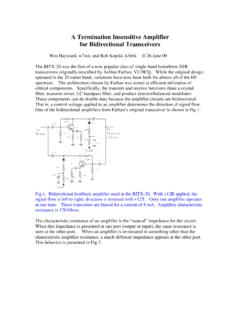
10 This is a stress rating only; functional operation of the product at these or any other conditions above those indicated in the operational section of this specification is not implied. Operation beyond the maximum operating conditions for extended periods may affect product reliability. ESD CAUTION data sheet AD8417 Rev. E | Page 5 of 17 PIN CONFIGURATIONS AND FUNCTION DESCRIPTIONS IN1 GND2 VREF23NC4+IN8 VREF17VS6 OUT5AD8417 TOP VIEW(Not to Scale) = NO CONNECT. DO NOTCONNECT TO THIS PIN. Figure 2. 8-Lead MSOP and 8-Lead SOIC_N Pin Configuration Table 4. 8-Lead MSOP and 8-Lead SOIC_N Pin Function Descriptions Pin No. Mnemonic Description 1 IN Negative Input. 2 GND Ground.