Transcription of 反応性スパッタリング法による Cr–N 作製とその特性
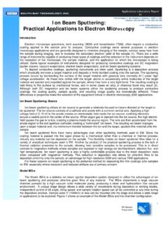
1 65 6 (2001)502 508. Cr N .. 1 2 2. 1 . 2 . J. Japan Inst. Metals, Vol. 65, No. 6 (2001), pp. 502 508. 2001 The Japan Institute of Metals Formation and Properties of Cr N Films by DC Reactive Sputtering Yukio Ide1, Hidenori Era2 and Katsuhiko Kishitake2. 1 Material Engineering Department, Yamaguchi Prefectural Industrial Technology Institute, Ube 755 0151. 2 Department of Materials Science and Engineering, Faculty of Engineering, Kyushu Institute of Technology, Kitakyushu 804 8550. Cr N films were deposited using a dc reactive sputtering apparatus equipped with an optical emission spectroscope(OES). and the behavior of some species excited in the plasma was monitored by OES during sputtering. The films deposited were characterized with respect to the chemical composition, crystal structure and wear resistance.
2 The results are summarized as fol- lows. (1) The N/Cr ratio monitored by OES increased proportionally with the nitrogen partial pressure. (2) The N/Cr ratio in the deposited films was nearly proportional to the N/Cr ratio measured by OES during sputtering. Therefore, it may be possible to control the chemical composition of Cr N films during sputtering. (3) The N/Cr ratio in the Cr N films increased continuously , and the structure of the films changed from Cr2N through Cr2N CrN to CrN with increasing nitrogen partial pressure. (4) Cr2O3 oxide surface layer was observed on the Cr N films after heating at 800 C for 60 min in air. (5) The crystal structure of CrN films hardly affected the friction coefficient at room temperature. The wear resistance of CrN single phase film was superior to Cr2N single phase film and Cr2N CrN dual phase film at 100 C.
3 (Received February 5, 2001; Accepted April 25, 2001). Keywords: optical emission spectroscopy, reactive sputtering, chromium nitride, hard coating, wear resistance TiN . 1. 9) Cr N . OES . Cr N Cr2N CrN Benien 10) . 1) . Cr N . Ti N Cr N. 2) Cr N OES . 3,4) MS . 2) Cr N Cr . Ti N . Chiba 5) . Cr N Ti N . Cr N Ti N 2.. Fig. 1 . ( OES) ( Cr N . MS ) 6 8) . 102 mm Cr . 1999 11 21 ( at ) . 6 Cr N 503. Fig. 1 Schematic diagram of reactive DC magnetron sputter - ing apparatus. Table 1 Experimental conditions for deposition of Cr N films. Sputtering power 300 W. Fig. 2 Typical spectra of chromium and nitrogen in sputter - Bias voltage 50 V ing. (sputtering power 300 W, argon partial pressure Ar partial pressure Pa Pa, nitrogen partial pressure Pa). N2 partial pressure Pa Substrate SUS304, SKH51. Substrate temperature 250.
4 C.. MS . OES MS . MS .. 11) MS . SUS304 100 mm 60 mm 2 mm N , N . 2 , Ar Cr . SKH51 20 mm 20 mm 4 mm Ti N 6) Al N 12) . (1 mm) SKH51 TiN AlN . SUS304 Cr N . 60 min CrN 250 . C. 10 3 Pa Gibbs . Ar 20 min TiN DG . 574 kJ mol 1, AlN DG . 526 kJ. Table 1 60 min mol 1 CrN DG . kJ mol 1 . Ti Al Cr . mm Ti Al . Cr .. Cr N . OES Pa . MS . Pa . Cr OES . 300 W Pa .. nm . Fig. 2 Cr N Cr . Ar Cr2N EPMA ZAF . Ar Cr . Cr N . 2 X . 429 nm . N . 2 392 nm, Ar 420 nm . 370 nm 440 nm . 3 . 504 (2001) 65 . Pa Cr . ( AES ) aJ aJ N EPMA . aJ N . 400 . C Cr EPMA . SKH51 N Cr N / Cr OES . N N Cr Fig. 5 . OES . Ti N 6) Ti Al N 8) Al . SKH51 Cr N 11) . 6 mm 100 . C OES . 5 N 100 mm /s . 100 m Enjouji 15) .. OES .. 3.. OES N Cr . Fig. 3 . 300 W Ar Pa . N/Cr .. Cr N .. Cr N .. Cr N Fig. 4 Relation between composition of Cr N films and nitro- gen partial pressure.
5 (sputtering power 300 W, argon partial Fig. 4 300 W Ar pressure Pa). Fig. 3 Relation between N/Cr ratio by OES and nitrogen par- Fig. 5 Relation between N/Cr ratio in films measured by tial pressure. (sputtering power 300 W, argon partial pres- EPMA and N/Cr ratio by OES during sputtering. (sputtering sure Pa). power 300 W, argon partial pressure Pa). 6 Cr N 505. 200 nm Pa . ( Fig. 7 (a )) . 300 W Ar Pa . Pa Pa Pa (Fig. 7 (c )) Pa . Cr N . Fig. 6 ( Fig. 7 ( b )) . Pa Cr N Fig. 7 (a ), ( d ). Pa 36 at N . Fig. 6 Cr2N . Fig. Pa 53 at N CrN. 7 Pa, Pa Pa N (Fig. 7 (c), ( f )) Pa . 36 at , 41 at , 53 at Cr N 41 at N CrN . CrN [001] . 10 .. Cr2N ( Fig. 7(b), (e)) . Fig. 8 X . Pa Cr2N. Pa Pa . CrN .. Fig. 8 X . Pa Pa 28 at N . 36 at N Cr2N Pa Pa 45 at N 53 at N. CrN . Fig. 6 Dark field image of the film deposited at a nitrogen par- Pa 41 at.
6 Tial pressure of Pa. The image was taken from the reflec- tion spots surrounded by a circle. Cr2N CrN Fig. 4 . Fig. 7 Selected area diffraction patterns (a through c) and indexed results (d through f). (a) and (c): PN2 Pa, (b) and (e): PN2 Pa, (c) and (f): PN2 Pa. 506 (2001) 65 . Fig. 9 Auger depth profile of CrN film deposited for 60 min. (sputtering power 300 W, nitrogen partial pressure Pa). Fig. 8 X ray diffraction patterns of Cr N films deposited in different nitrogen partial pressures. (sputtering power 300. W, argon partial pressure Pa). N at . Cr2N Cr2N CrN . CrN Pa Pa . Cr2N (11 20) .. N . Cr2N . Pa CrN . Pa . CrN . Cr N . 13) Cr2N CrN Fig. 10 Auger depth profile of CrN film held at 800 . C for 60. min in air. 50 at N 45. at N 53 at N CrN . 14) CrN . N 55 at N .. Cr2N CrN N .. Pa CrN 400 . C, PN Pa CrN AES.
7 2. 600 . C 800 . C 60 min X . Fig. 9 Cr N Fig. 11 400 . C CrN . 600 . C CrN Cr . mm 450 min . mm Fig. 10 800 . C CrN Cr2O3 . 800 . C 60 min Cr2O3 . Cr CrN 2 AES . 2) . CrN . 6 Cr N 507. Fig. 12 Knoop hardness of Cr N films measured at a load of N as a function of temperature. Fig. 11 X ray diffraction patterns of CrN film held at 400 . C, 600 C and 800 . C for 60 min in air, respectively.. Cr2N(36 at N), CrN Cr2N(41 at N). CrN ( 45 at N ) 20 . C . 400 . C Fig. 12 .. Cr2N CrN . CrN CrN Cr2N . CrN Cr2N .. Fig. 13 Friction coefficient of Cr N films measured by ball . on disc wear test.. Cr N . Benien 10) Cr2N CrN Cr2N . Bull 16) 5) 100 . C . CrN 100 . C . 20 . C .. 14) 17) 100 . C Cr2N . 22 m Cr2N CrN 7 m . Cr N . 100 . C . Cr2N CrN CrN Cr2N Cr2N CrN . Cr2N 20 . C 100 . C CrN . Fig. 13 20 . C Cr2N Cr2N CrN.
8 CrN .. CrN . 508 (2001) 65 . 4.. Cr N 1) W. Dong Dong and T. Oki: Hyomen Gijutsu 40(1989) 96 97. 2) A. Kawana and H. Ichimura: Shigen to Sozai 108(1992) 868 . OES 872. 3) M. Taguchi and H. Takahashi: Mater. Trans., JIM 35(1994). 356 362. 4) S. Ohtani, T. Takagi and C. Yanagi: Hyomen Gijutsu 43(1992). 1168 1171. 5) Y. Chiba, T. Omura and H. Ichimura: J. Mater. Res. 8(1993). 1109 1115.. (OES) N Cr 6) Y. Ide and T. Nakamura: J. Japan Inst. Metals 57(1993). 926 931. 7) Y. Ide, Y. Kawasaki and T. Nakamura: Metallurgical Proc. for Early Twenty First Century, ed. by H. Y. Sohn, (TMS, 1994).. EPMA N Cr OES . 121 130. N Cr 8) Y. Ide, K. Inada, T. Nakamura and M. Maeda: J. Japan Inst. Metals 62(1998) 98 105. OES 9) S. Inoue, H. Uchida, A. Hioki and K. Koterazawa: J. Japan Inst. Metals 60(1996) 1090 1094. 10) H.
9 Benien, J. Maushart, M. Meyer and R. Suchentrunk: Mater.. Sci. Eng. A139(1991) 126 131. Cr2N Cr2N 11) Y. Ide, K. Kishitake and T. Nakamura: J. Japan Inst. Metals 63(1999) 1576 1583. CrN CrN 12) M. Ishihara, S. J. Li, H. Yumoto, K. Akashi and Y. Ide: Thin . Cr Solid Films 316(1998) 152 157. 13) G. Bertrand, C. Savall and C. Meunier: Surface Engineering CrN 2 Cr 14(1998) 246 249. 14) K. Yamamoto, F. Yuse, T. Nakayama and F. Kamikubo: Cr2O3 . Hyomen Gijutsu 48(1997) 446 453.. Cr N 15) K. Enjouji, K. Murata and S. Nishikawa: Thin Solid Films 108(1983) 1 7. 100 . C CrN Cr2N 16) S. J. Bull and D. S. Rickerby: Surface and Coatings Technology Cr2N CrN 43/44(1990) 732 744. 17) Y. Enomoto and S. Miyake: Tribology of Thin Films, (Universi- ty of Tokyo Press, Tokyo, 1994) pp. 77 84.