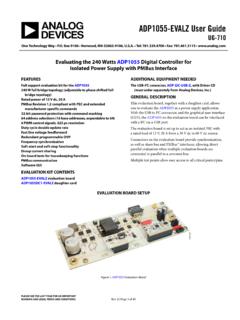
Transcription of Digital Controller for Power Supply Applications …
1 Digital Controller for Power Supply Applications with PMBus interface Data Sheet ADP1055. FEATURES Extended black box data recorder for fault recording 40 C to +125 C operation User trimming on input and output voltages and currents PMBus Revision compliant with PEC and extended Digital current sharing manufacturer specific commands Applications . 32-bit password protection with command masking Isolated dc-to-dc Power supplies and modules 64 address selections (16 base addresses, expandable to 64). Redundant Power Supply systems 6 PWM control signals, 625 ps resolution Frequency from 48 kHz to 1 MHz GENERAL DESCRIPTION.
2 Duty cycle double update rate The ADP1055 is a flexible, feature-rich Digital secondary side Digital control loop (PID + additional pole or zero Controller that targets ac-to-dc and isolated dc-to-dc secondary configurability) side Applications . The ADP1055 is optimized for minimal Programmable loop filters (CCM, DCM, low/normal component count, maximum flexibility, and minimum design temperature) time. Features include differential remote voltage sense, primary Fast line voltage feedforward and secondary side current sense, pulse-width modulation (PWM).
3 Adaptive dead time compensation for improved efficiency generation, frequency synchronization, redundant OVP, and Remote voltage sense current sharing. The control loop Digital filter and compensation Redundant programmable OVP. terms are integrated and can be programmed over the PMBus . Current sense interface . Programmable protection features include Primary side cycle-by-cycle fast protection overcurrent (OCP), overvoltage (OVP) limiting, undervoltage Secondary side cycle-by-cycle fast overcurrent protection lockout (UVLO), and external overtemperature (OTP).
4 Secondary side averaged reverse current protection using diode emulation mode with fixed debounce The built-in EEPROM provides extensive programming of the Synchronous rectifier control for improved efficiency integrated loop filter, PWM signal timing, inrush current, and in light load mode soft start timing and sequencing. Reliability is improved through Nonlinear gain for faster transient response from DCM to CCM a built-in checksum and programmable protection circuits. Frequency synchronization A comprehensive GUI is provided for easy design of loop filter Soft start and soft stop functionality characteristics and programming of the safety features.
5 The Average and peak constant current mode industry-standard PMBus provides access to the many monitoring External PN junction temperature sensing and system test functions. The ADP1055 is available in a 32-lead 4 GPIOs (2 GPIOs configurable as active clamp snubber PWMs) LFCSP and operates from a single V Supply . TYPICAL APPLICATION DIAGRAM. VOUT. DC. INPUT. LOAD. DRIVER. SR1 SR2 VFF CS2 CS2+ OVP VS+ VS . CS1. ISHARE. OUTA. OUTB SYNC. DRIVER iCoupler OUTC. ADP1055. NC. OUTD. VCORE. RES ADD JTD JRTN GPIO1 TO GPIO4 CTRL SMBALRT SDA SCL VDD AGND DGND.
6 VDD. 12004-001. PMBus Figure 1. Rev. A Document Feedback Information furnished by analog devices is believed to be accurate and reliable. However, no responsibility is assumed by analog devices for its use, nor for any infringements of patents or other rights of third parties that may result from its use. Specifications subject to change without notice. No One Technology Way, Box 9106, Norwood, MA 02062-9106, license is granted by implication or otherwise under any patent or patent rights of analog devices . Tel: 2014 2015 analog devices , Inc.
7 All rights reserved. Trademarks and registered trademarks are the property of their respective owners. Technical Support ADP1055 Data Sheet TABLE OF CONTENTS. Features .. 1 Matched Cycle-by-Cycle Current Limit (OCP Equalization) .. 25. Applications .. 1 Low Temperature Filter .. 25. General Description .. 1 Voltage Loop Autocorrection .. 25. Typical Application Diagram .. 1 Nonlinear Gain/Response .. 26. Revision History .. 3 Integrator Windup and Output Voltage Regulation Loss Functional Block Diagram .. 4 (Overshoot Protection) .. 26.
8 5 Accurate Secondary Overcurrent Protection .. 26. Absolute Maximum 10 Secondary Fast Overcurrent Protection .. 27. Thermal Resistance .. 10 Secondary Fast Reverse Current 27. Soldering .. 10 Feedforward and Input Voltage Sense .. 27. ESD Caution .. 10 Accurate Overvoltage and Undervoltage 28. Pin Configuration and Function Descriptions .. 11 Fast Overvoltage 28. Typical Performance Characteristics .. 13 External Frequency Synchronization .. 28. Controller Architecture .. 16 Temperature Sensing .. 29. Start-Up and Power -Down Sequencing.
9 17 GPIO and PGOOD Signals .. 29. VDD and VCORE 17 GPIO3 and GPIO4 as Snubber PWM Outputs .. 31. Power -Up and Power -Down Commands .. 17 Average Constant Current Mode .. 32. Power Sequencing .. 17 32-Bit Key Code .. 32. Power -Up and Soft Start Routine .. 17 SR Phase-In, SR Transition, and SR Fast Phase-In .. 33. Soft Stop Routine .. 17 Output Voltage Slew Rate .. 33. VDD/VCORE OVLO .. 18 Adaptive Dead Time Compensation .. 33. Control Loop and PWM 19 SR Delay .. 34. Voltage Sense, Feedback, and Control 19 Current Sharing (ISHARE Pin) .. 34.
10 Output Voltage Sense .. 19 Droop Sharing .. 36. Digital Filter .. 19 Light Load Mode and Deep Light Load Mode .. 37. Digital Filter Programming Registers .. 20 Pulse 37. Digital Compensation Filters During Soft 20 Soft Stop .. 37. Filter Transition .. 20 Duty Cycle Double Update Rate .. 37. PWM and Synchronous Rectifier Outputs (OUTA, OUTB, Duty Balance, Volt-Second Balance, and Flux Balancing .. 38. OUTC, OUTD, SR1, SR2) .. 21 Fault Responses and State Machine Mechanics .. 39. Synchronous Rectification .. 21 Priority of Faults .. 39. Modulation Limit.
