Transcription of Digital Output MEMS Accelerometer Data Sheet …
1 Micropower, 3-Axis, 2 g/ 4 g/ 8 g Digital Output MEMS Accelerometer data Sheet adxl362 Rev. E Document Feedback Information furnished by analog devices is believed to be accurate and reliable. However, no responsibility is assumed by analog devices for its use, nor for any infringements of patents or other rights of third parties that may result from its use. Specifications subject to change without notice. No license is granted by implication or otherwise under any patent or patent rights of analog devices .
2 Trademarks and registered trademarks are the property of their respective owners. One Technology Way, Box 9106, Norwood, MA 02062-9106, Tel: 2012 2016 analog devices , Inc. All rights reserved. Technical Support FEATURES Ultralow power Power can be derived from coin cell battery A at 100 Hz ODR, V supply A at 400 Hz ODR, V supply 270 nA motion activated wake-up mode 10 nA standby current High resolution: 1 mg/LSB Built-in features for system-level power savings: Adjustable threshold sleep/wake modes for motion activation Autonomous interrupt processing, without need for microcontroller intervention, to allow the rest of the system to be turned off completely Deep embedded FIFO minimizes host processor load Awake state Output enables implementation of standalone, motion activated switch Low noise down to 175 g/ Hz Wide supply and I/O voltage ranges.
3 V to V Operates off V to V rails Acceleration sample synchronization via external trigger On-chip temperature sensor SPI Digital interface Measurement ranges selectable via SPI command Small and thin 3 mm mm mm package APPLICATIONS Hearing aids Home healthcare devices Motion enabled power save switches Wireless sensors Motion enabled metering devices GENERAL DESCRIPTION The adxl362 is an ultralow power, 3-axis MEMS Accelerometer that consumes less than 2 A at a 100 Hz Output data rate and 270 nA when in motion triggered wake-up mode.
4 Unlike accelerometers that use power duty cycling to achieve low power consumption, the adxl362 does not alias input signals by undersampling; it samples the full bandwidth of the sensor at all data rates. The adxl362 always provides 12-bit Output resolution; 8-bit formatted data is also provided for more efficient single-byte transfers when a lower resolution is sufficient. Measurement ranges of 2 g, 4 g, and 8 g are available, with a resolution of 1 mg/LSB on the 2 g range. For applications where a noise level lower than the normal 550 g/ Hz of the adxl362 is desired, either of two lower noise modes (down to 175 g/ Hz typical) can be selected at minimal increase in supply current.
5 In addition to its ultralow power consumption, the adxl362 has many features to enable true system level power reduction. It includes a deep multimode Output FIFO, a built-in micropower temperature sensor, and several activity detection modes including adjustable threshold sleep and wake-up operation that can run as low as 270 nA at a 6 Hz (approximate) measurement rate. A pin Output is provided to directly control an external switch when activity is detected, if desired. In addition, the adxl362 has provisions for external control of sampling time and/or an external clock.
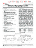
6 The adxl362 operates on a wide V to V supply range, and can interface, if necessary, to a host operating on a separate, lower supply voltage. The adxl362 is available in a 3 mm mm mm package. FUNCTIONAL BLOCK DIAGRAM VSVDDI/OGND3-AXISMEMSSENSORTEMPERATURESE NSORAXISDEMODULATORSANTIALIASINGFILTERSA DXL36212-BITADCDIGITALLOGIC,FIFO,ANDSPII NT1 INT2 MOSIMISOCSSCLK10776-001 Figure 1. adxl362 data Sheet Rev. E | Page 2 of 43 TABLE OF CONTENTS Features .. 1 Applications .. 1 General Description .. 1 Functional Block Diagram.
7 1 Revision History .. 3 Specifications .. 4 Absolute Maximum Ratings .. 6 Thermal Resistance .. 6 Package Information .. 6 Recommended Soldering Profile .. 6 ESD Caution .. 6 Pin Configuration and Function Descriptions .. 7 Typical Performance Characteristics .. 8 Theory of Operation .. 13 Mechanical Device Operation .. 13 Operating Modes .. 13 Selectable Measurement Ranges .. 13 Selectable Output data Rates .. 13 Power/Noise Tradeoff .. 14 Power Savings Features .. 15 Ultralow Power Consumption in All Modes.
8 15 Motion Detection .. 15 FIFO .. 17 Communications .. 17 Additional Features .. 18 Free Fall Detection .. 18 External Clock .. 18 Synchronized data Sampling .. 18 Self Test .. 18 User Register Protection .. 18 Temperature Sensor .. 18 Serial Communications .. 19 SPI Commands .. 19 Multibyte Transfers .. 19 Invalid Addresses and Address Folding .. 19 Latency Restrictions .. 19 Invalid Commands .. 19 Register Map .. 23 Register Details .. 24 Device ID Register .. 24 Device ID: 0x1D Register .. 24 Part ID: 0xF2 Register.
9 24 Silicon Revision ID Register .. 24 X-Axis data (8 MSB) Register .. 24 Y-Axis data (8 MSB) Register .. 24 Z-Axis data (8 MSB) Register .. 24 Status Register .. 25 FIFO Entries Registers .. 26 X-Axis data Registers .. 26 Y-Axis data Registers .. 26 Z-Axis data Registers .. 26 Temperature data Registers .. 26 Soft Reset Register .. 26 Activity Threshold Registers .. 27 Activity Time Register .. 27 Inactivity Threshold Registers .. 27 Inactivity Time Registers .. 27 Activity/Inactivity Control Register .. 29 FIFO Control Register.
10 30 FIFO Samples Register .. 31 INT1/INT2 Function Map Registers .. 31 Filter Control Register .. 33 Power Control 34 Self Test Register .. 35 Applications Information .. 36 Application Examples .. 36 37 FIFO Modes .. 38 Interrupts .. 39 Using Synchronized data Sampling .. 40 Using an External Clock .. 41 Using Self Test .. 41 Operation at Voltages Other Than V .. 41 Mechanical Considerations for Mounting .. 41 Axes of Acceleration Sensitivity .. 42 Layout and Design Recommendations .. 42 Outline Dimensions.