Transcription of DS21373C - Microchip Technology
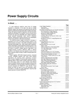
1 tc1262 . 500mA Fixed Output CMOS LDO. Features Package Type Very Low Dropout Voltage 3-Pin TO-220 3-Pin DDPAK. 500mA Output Current Front View High Output Voltage Accuracy Tab is GND Tab is GND. Standard or Custom Output Voltages Over Current and Over Temperature Protection tc1262 tc1262 . Applications 3 1 2 3. 1 2. Battery Operated Systems Portable Computers 3-Pin SOT-223. VIN. GND. VOUT. VIN. GND. VOUT. Medical Instruments Front View Instrumentation Cellular/GSM/PHS Phones 3 VOUT. Linear Post-Regulators for SMPS. Tab is GND. Pagers 2 GND. Device Selection Table 1 VIN. tc1262 . Junction Part Number Package Temp. Range General Description tc1262 -xxVDB 3-Pin SOT-223 -40 C to +125 C. The tc1262 is a fixed output, high accuracy (typically tc1262 -xxVAB 3-Pin TO-220 -40 C to +125 C.)
2 CMOS low dropout regulator. Designed specif- tc1262 -xxVEB 3-Pin DDPAK -40 C to +125 C ically for battery-operated systems, the tc1262 's CMOS construction eliminates wasted ground current, NOTE: xx indicates output voltages. significantly extending battery life. Total supply current Available Output Voltages: , , , , is typically 80 A at full load (20 to 60 times lower than Other output voltages are available. Please contact Microchip in bipolar regulators). Technology Inc. for details. tc1262 key features include ultra low noise operation, very low dropout voltage (typically 350mV at full load), and fast response to step changes in load. The tc1262 incorporates both over temperature and over current protection.
3 The tc1262 is stable with an output capacitor of only 1 F and has a maximum output current of 500mA. It is available in 3-Pin SOT-223, 3-Pin TO-220 and 3-Pin DDPAK packages. Typical Application VIN VIN VOUT VOUT. +. C1. tc1262 1 F. GND. 2002-2012 Microchip Technology Inc. DS21373C -page 1. tc1262 . ELECTRICAL *Stresses above those listed under "Absolute Maximum Ratings" may cause permanent damage to the device. These CHARACTERISTICS are stress ratings only and functional operation of the device at these or any other conditions above those indicated in the Absolute Maximum Ratings*. operation sections of the specifications is not implied. Input Voltage .. Exposure to Absolute Maximum Rating conditions for extended periods may affect device reliability.
4 Output (VSS ) to (VIN + ). Power Limited (Note 6). Maximum Voltage on Any Pin ..VIN + to Operating Temperature -40 C < TJ < 125 C. Storage C to +150 C. tc1262 ELECTRICAL SPECIFICATIONS. Electrical Characteristics: VIN = VOUT + 1V, IL = 100 A, CL = F, TA = 25 C, unless otherwise noted. Boldface type specifications apply for junction temperatures of -40 C to +125 C. Symbol Parameter Min Typ Max Units Test Conditions VIN Input Operating Voltage V Note 7. IOUTMAX Maximum Output Current 500 mA. VOUT Output Voltage VR V Note 1. VR VR + VOUT/ T VOUT Temperature Coefficient 40 ppm/ C Note 2. VOUT/ VIN Line Regulation .003 %/V (VR + 1V) VIN 6V. VOUT/VOUT Load Regulation %/mA IL = to IOUTMAX (Note 3).
5 VIN-VOUT Dropout Voltage 20 30 mV IL = 100 A. 60 130 IL = 100mA. 200 390 IL = 300mA. 350 650 IL = 500mA (Note 4). IDD Supply Current 80 130 A IL = 0. PSRR Power Supply Rejection Ratio 64 dB FRE 1kHz IOUTSC Output Short Circuit Current 1200 mA VOUT = 0V. VOUT/ PD Thermal Regulation V/W Note 5. eN Output Noise 260 nV/ Hz IL = IOUTMAX, FRE = 10kHz Note 1: VR is the regulator output voltage setting. 2: TC VOUT = (VOUTMAX VOUTMIN) x 106. VOUT x T. 3: Regulation is measured at a constant junction temperature using low duty cycle pulse testing. Load regulation is tested over a load range from to the maximum specified output current. Changes in output voltage due to heating effects are covered by the thermal regulation specification.
6 4: Dropout voltage is defined as the input to output differential at which the output voltage drops 2% below its nominal value measured at a 1V differential. 5: Thermal Regulation is defined as the change in output voltage at a time T after a change in power dissipation is applied, excluding load or line regulation effects. Specifications are for a current pulse equal to ILMAX at VIN = 6V for T = 10 msec. 6: The maximum allowable power dissipation is a function of ambient temperature, the maximum allowable junction temperature and the thermal resistance from junction-to-air ( , TA, TJ, JA). Exceeding the maximum allowable power dissipation causes the device to initiate thermal shutdown.
7 Please see Section Thermal Considerations for more details. 7: The minimum VIN has to justify the conditions: VIN VR + VDROPOUT and VIN for IL = to IOUTMAX. DS21373C -page 2 2002-2012 Microchip Technology Inc. tc1262 . PIN DESCRIPTIONS. The descriptions of the pins are listed in Table 2-1. TABLE 2-1: PIN FUNCTION TABLE. Pin No. (3-Pin SOT-223). Symbol Description (3-Pin TO-220). (3-Pin DDPAK). 1 VIN Unregulated supply input. 2 GND Ground terminal. 3 VOUT Regulated voltage output. DETAILED DESCRIPTION Output Capacitor The tc1262 is a precision, fixed output LDO. Unlike A 1 F (min) capacitor from VOUT to ground is required. bipolar regulators, the tc1262 's supply current does The output capacitor should have an effective series not increase with load current.
8 In addition, VOUT resistance greater than and less than 5 , and a remains stable and within regulation over the entire resonant frequency above 1 MHz. A 1 F capacitor 0mA to ILOADMAX load current range (an important should be connected from VIN to GND if there is more consideration in RTC and CMOS RAM battery back-up than 10 inches of wire between the regulator and the applications). AC filter capacitor, or if a battery is used as the power source. Aluminum electrolytic or tantalum capacitor Figure 3-1 shows a typical application circuit. types can be used. (Since many aluminum electrolytic capacitors freeze at approximately -30 C, solid FIGURE 3-1: TYPICAL APPLICATION tantalums are recommended for applications operating CIRCUIT below -25 C.)
9 When operating from sources other than batteries, supply-noise rejection and transient VIN VOUT VOUT response can be improved by increasing the value of + +. C1 C2 the input and output capacitors and employing passive + 1 F tc1262 1 F. Battery filtering techniques. GND.. 2002-2012 Microchip Technology Inc. DS21373C -page 3. tc1262 . THERMAL CONSIDERATIONS TABLE 4-2: THERMAL RESISTANCE. GUIDELINES FOR tc1262 IN. Thermal Shutdown 3-PIN DDPAK/TO-220. PACKAGE. Integrated thermal protection circuitry shuts the regulator off when die temperature exceeds 160 C. Copper Copper Thermal The regulator remains off until the die temperature Board Area Area Resistance drops to approximately 150 C.
10 Area (Topside)* (Backside) JA). Power Dissipation 2500 sq mm 2500 sq mm 2500 sq mm 25 C/W. 1000 sq mm 2500 sq mm 2500 sq mm 27 C/W. The amount of power the regulator dissipates is primarily a function of input and output voltage, and 125 sq mm 2500 sq mm 2500 sq mm 35 C/W. output current. The following equation is used to *Tab of device attached to topside copper calculate worst case actual power dissipation: Equation 4-1 can be used in conjunction with Equation EQUATION 4-1: 4-2 to ensure regulator thermal operation is within limits. For example: PD (VINMAX VOUTMIN)ILOADMAX. Given: Where: VINMAX = 10%. PD = Worst case actual power dissipation VINMAX = Maximum voltage on VIN VOUTMIN = VOUTMIN = Minimum regulator output voltage ILOADMAX = 275mA.