Transcription of Dual-Channel, 2.5 kV Isolators with Integrated DC …
1 dual - channel , kV Isolators with Integrated DC-to-DC ConverterData sheet adum5200 / adum5201 / adum5202 Rev. B Information furnished by analog devices is believed to be accurate and reliable. However, no responsibility is assumed by analog devices for its use, nor for any infringements of patents or other rights of third parties that may result from its use. Specifications subject to change without notice. No license is granted by implication or otherwise under any patent or patent rights of analog devices . Trademarks and registered trademarks are the property of their respective owners. One Technology Way, Box 9106, Norwood, MA 02062-9106, : Fax: 2009-2012 analog devices , Inc.
2 All rights reserved. FEATURES isoPower Integrated , isolated dc-to-dc converter Regulated V or 5 V output Up to 500 mW output power dual , dc-to-25 Mbps (NRZ) signal isolation channels 16-lead SOIC package with mm creepage High temperature operation: 105 C maximum High common-mode transient immunity: >25 kV/ s Safety and regulatory approvals UL recognition 2500 V rms for 1 minute per UL 1577 CSA Component Acceptance Notice #5A) VDE certificate of conformity (pending) IEC 60747-5-2 (VDE 0884, Part 2):2003-01 VIORM = 560 VPEAK APPLICATIONS RS-232/RS-422/RS-485 transceivers Industrial field bus isolation Power supply start-up bias and gate drives Isolated sensor interfaces Industrial PLCs GENERAL DESCRIPTION The adum5200 / adum5201 /ADuM52021 are dual - channel digital Isolators with isoPower , an Integrated , isolated dc-to-dc converter .
3 Based on the analog devices , Inc., iCoupler technology, the dc-to-dc converter provides up to 500 mW of regulated, isolated power at either V or V from a V input supply, or V from a V supply at the power levels shown in Table 1. These devices eliminate the need for a separate, isolated dc-to-dc converter in low power isolated designs. The iCoupler chip scale transformer technology is used to isolate the logic signals and for the magnetic components of the dc-to-dc converter . The result is a small form factor, total isolation solution. The adum5200 / adum5201 / adum5202 Isolators provide two independent isolation channels in a variety of channel configurations and data rates (see the Ordering Guide for more information).
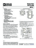
4 IsoPower uses high frequency switching elements to transfer power through its transformer. Special care must be taken during printed circuit board (PCB) layout to meet emissions standards. See the AN-0971 Application Note for board layout recommendations. FUNCTIONAL BLOCK DIAGRAMS 12345678161514131211109 OSCRECT2-CHANNELiCOUPLER COREVDD1 REGGND1 VIA/VOAVIB/VOBRCINRCSELVE1/NCGND1 VISOGNDISOVIA/VOAVIB/VOBNCVSELVE2/NCGNDI SOADuM5200/ adum5201 /ADuM520207540-001 Figure 1. 341413 ADuM520007540-002 VIAVIBVOAVOB Figure 2. adum5200 341413 ADuM520107540-003 VIAVOBVOAVIB Figure 3. adum5201 341413 ADuM520207540-004 VOAVOBVIAVIB Figure 4. adum5202 Table 1. Power Levels Input Voltage (V) Output Voltage (V) Output Power (mW) 500 330 200 1 Protected by Patents 5,952,849; 6,873,065; 6,903,578; and 7,075,329.
5 adum5200 / adum5201 / adum5202 data sheet Rev. B | Page 2 of 28 TABLE OF CONTENTS Features .. 1 Applications .. 1 General Description .. 1 Functional Block Diagrams .. 1 Revision History .. 2 Specifications .. 3 Electrical Characteristics 5 V Primary Input Supply/ 5 V Secondary Isolated Supply .. 3 Electrical Characteristics V Primary Input Supply/ V Secondary Isolated Supply .. 5 Electrical Characteristics 5 V Primary Input Supply/ V Secondary Isolated Supply .. 7 Package Characteristics .. 9 Regulatory Information .. 9 Insulation and Safety-Related Specifications .. 9 IEC 60747-5-2 (VDE 0884, Part 2):2003-01 Insulation Characteristics .. 10 Recommended Operating Conditions .. 10 Absolute Maximum Ratings.
6 11 ESD Caution .. 11 Pin Configurations and Function Descriptions .. 12 Tr u t h Ta b l e .. 14 Typical Performance Characteristics .. 15 Terminology .. 18 Applications Information .. 19 PCB Layout .. 19 Start-Up 19 EMI Considerations .. 20 Propagation Delay Parameters .. 20 DC Correctness and Magnetic Field 20 Power Consumption .. 21 Current Limit and Thermal Overload Protection .. 22 Power Considerations .. 22 Thermal Analysis .. 23 Increasing Available Power .. 23 Insulation Lifetime .. 24 Outline Dimensions .. 25 Ordering Guide .. 25 REVISION HISTORY 5/12 Rev. A to Rev. B Created Hyperlink for Safety and Regulatory Approvals Entry in Features Section .. 1 Updated Outline Dimensions.
7 25 9/11 Rev. 0 to Rev. A Changes to Product Title, Features Section, and General Description Section .. 1 Added Table 1; Renumbered Sequentially .. 1 Changes to Specifications Section .. 3 Changes to Table 19 and Table 20 .. 11 Changes to Pin 5 Description, Table 21 .. 12 Changes to Pin 5 Description, Table 22 .. 13 Changes to Pin 5 Description, Table 23 and Ta b l e 2 4 .. 14 Changes to Figure 9 to Figure 11 .. 15 Added Figure 17 and Figure 18; Renumbered Sequentially .. 16 Changes to Figure 19 and Figure 20 .. 16 Changes to Terminology Section .. 18 Changes to Applications Information Section .. 19 Added Start-Up Behavior Section .. 19 Changes to EMI Considerations Section .. 20 10/08 Revision 0: Initial Version data sheet adum5200 / adum5201 / adum5202 Rev.
8 B | Page 3 of 28 SPECIFICATIONS ELECTRICAL CHARACTERISTICS 5 V PRIMARY INPUT SUPPLY/5 V SECONDARY ISOLATED SUPPLY All typical specifications are at TA = 25 C, VDD1 = VSEL = VISO = 5 V. Minimum/maximum specifications apply over the entire recommended operation range which is V VDD1, VSEL, VISO V; and 40 C TA +105 C, unless otherwise noted. Switching specifications are tested with CL = 15 pF and CMOS signal levels, unless otherwise noted. Table 2. DC-to-DC converter Static Specifications Parameter Symbol Min Typ Max Unit Test Conditions DC-TO-DC converter SUPPLY Setpoint VISO V IISO = 0 mA Line Regulation VISO (LINE) 1 mV/V IISO = 50 mA, VDD1 = V to V Load Regulation VISO (LOAD) 1 5 % IISO = 10 mA to 90 mA Output Ripple VISO (RIP) 75 mV p-p 20 MHz bandwidth, CBO = F||10 F, IISO = 90 mA Output Noise VISO (NOISE) 200 mV p-p CBO = F||10 F, IISO = 90 mA Switching Frequency fOSC 180 MHz PW Modulation Frequency fPWM 625 kHz Output Supply IISO (MAX) 100 mA VISO > V Efficiency at IISO (MAX) 34 % IISO = 100 mA IDD1, No VISO Load IDD1 (Q) 8 22 mA IDD1, Full VISO Load IDD1 (MAX)
9 290 mA Table 3. DC-to-DC converter Dynamic Specifications Parameter Symbol 1 Mbps A Grade or C Grade 25 Mbps C Grade Unit Test Conditions Min Typ Max Min Typ Max SUPPLY CURRENT Input No VISO load adum5200 IDD1 6 34 mA adum5201 IDD1 7 38 mA adum5202 IDD1 7 41 mA Available to Load adum5200 IISO (LOAD) 100 94 mA adum5201 IISO (LOAD) 100 92 mA adum5202 IISO (LOAD) 100 90 mA Table 4. Switching Specifications Parameter Symbol A Grade C Grade Unit Test Conditions Min Typ Max Min Typ Max SWITCHING SPECIFICATIONS data Rate 1 25 Mbps Within PWD limit Propagation Delay tPHL, tPLH 55 100 45 60 ns 50% input to 50% output Pulse Width Distortion PWD 40 6 ns |tPLH tPHL| Change vs.
10 Temperature 5 ps/ C Pulse Width PW 1000 40 ns Within PWD limit Propagation Delay Skew tPSK 50 15 ns Between any two units channel Matching Codirectional1 tPSKCD 50 6 ns Opposing Directional2 tPSKOD 50 15 ns 1 7 Codirectional channel matching is the absolute value of the difference in propagation delays between any two channels with inputs on the same side of the isolation barrier. 2 Opposing directional channel matching is the absolute value of the difference in propagation delays between any two channels with inputs on opposing sides of the isolation barrier. adum5200 / adum5201 / adum5202 data sheet Rev. B | Page 4 of 28 Table 5. Input and Output Characteristics Parameter Symbol Min Typ Max Unit Test Conditions DC SPECIFICATIONS Logic High Input Threshold VIH VISO or VDD1 V Logic Low Input Threshold VIL VISO or VDD1 V Logic High Output Voltages VOH VDD1 or VISO V IOx = 20 A, VIx = VIxH VDD1 or VISO V IOx = 4 mA, VIx = VIxH Logic Low Output Voltages VOL V IOx = 20 A, VIx = VIxL V IOx = 4 mA, VIx = VIxL Undervoltage Lockout VDD1, VDDL.
