Transcription of Dual Differential 16-Bit, 1 MSPS PulSAR ADC 12.0 mW in ...
1 dual Differential 16-Bit, 1 msps . PulSAR ADC mW in QSOP. Data Sheet AD7903. FEATURES GENERAL DESCRIPTION. 16-bit resolution with no missing codes The AD7903 is a dual 16-bit, successive approximation, analog- Throughput: 1 msps to-digital converter (ADC) that operates from a single power Low power dissipation supply, VDDx, per ADC. It contains two low power, high speed, mW at 1 msps (VDD1 and VDD2 only) 16-bit sampling ADCs and a versatile serial port interface (SPI). mW at 1 msps (total) On the CNVx rising edge, the AD7903 samples the voltage 140 W at 10 kSPS difference between the INx+ and INx pins.
2 The voltages on INL: LSB typical, LSB maximum these pins usually swing in opposite phases between 0 V and SINAD: dB at 1 kHz VREF. The externally applied reference voltage of the REFx pins THD: 112 dB at 1 kHz (VREF) can be set independently from the supply voltage pins, True Differential analog input range: VREF VDDx. The power of the device scales linearly with throughput. 0 V to VREF with VREF between V to V. Using the SDIx inputs, the SPI-compatible serial interface can Allows use of any input range also daisy-chain multiple ADCs on a single 3-wire bus and provide Easy to drive with the ADA4941-1.
3 An optional busy indicator. It is compatible with V, V, 3 V, No pipeline delay or 5 V logic, using the separate VIOx supplies. Single-supply V operation with V/3 V/5 V logic interface The AD7903 is available in a 20-lead QSOP package with operation Serial port interface (SPI)/QSPI/MICROWIRE/DSP compatible specified from 40 C to +125 C. 20-lead QSOP package Table 1. MSOP 14-/16-/18-Bit PulSAR ADCs Wide operating temperature range: 40 C to +125 C 100 250 400 kSPS 1000 ADC. Bits kSPS kSPS to 500 kSPS kSPS Driver APPLICATIONS 18 AD76911 AD76901 AD79821 ADA4941-1.
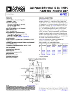
4 Battery-powered equipment ADA4841-x Communications 16 AD7680 AD76851 AD76861 AD79801 ADA4941-1. Automated test equipment (ATE) AD7683 AD76871 AD76881 AD7903 ADA4841-x Data acquisition AD7684 AD7694 AD76931 AD7902. Medical instrumentation 14 AD7940 AD79421 AD79461. Redundant measurement 1. Pin-for-pin compatible. Simultaneous sampling FUNCTIONAL BLOCK DIAGRAM. REF = TO 5V. REF1 REF2 VDD1 VDD2. ADA4941-1. VIO1 VIO1/VIO2. REF IN1+. SDI1 SDI1/SDI2. ADC1 SCK1 SCK1/SCK2. CNV1 CNV1/CNV2. 10V, 5V, .. IN1 . SDO1 SDO1. ADA4941-1. VIO2.
5 REF IN2+ 3-WIRE OR 4-WIRE. SDI2 INTERFACE. ADC2 SCK2 (SPI, CS, AND. CHAIN MODES). CNV2. 10V, 5V, .. IN2 . SDO2 SDO2. GND AD7903. 11755-001. Figure 1. Rev. B Document Feedback Information furnished by Analog Devices is believed to be accurate and reliable. However, no responsibility is assumed by Analog Devices for its use, nor for any infringements of patents or other rights of third parties that may result from its use. Specifications subject to change without notice. No One Technology Way, Box 9106, Norwood, MA 02062-9106, license is granted by implication or otherwise under any patent or patent rights of Analog Devices.
6 Tel: 2013 2014 Analog Devices, Inc. All rights reserved. Trademarks and registered trademarks are the property of their respective owners. Technical Support AD7903 Data Sheet TABLE OF CONTENTS. Features .. 1 Analog 15. Applications .. 1 Driver Amplifier Choice .. 16. General Description .. 1 Single-to- Differential Driver .. 16. Functional Block Diagram .. 1 Voltage Reference Input .. 17. Revision History .. 2 Power 17. 3 Digital Interface .. 17. Timing Specifications .. 5 CS Mode .. 18. Absolute Maximum Ratings .. 6 Chain Mode.
7 22. ESD Caution .. 6 Applications Information .. 24. Pin Configuration and Function Descriptions .. 7 Simultaneous Sampling .. 24. Typical Performance Characteristics .. 8 Functional Safety Considerations .. 25. Terminology .. 13 26. Theory of Operation .. 14 Evaluating Performance of the 26. Circuit Information .. 14 Outline Dimensions .. 27. Converter Operation .. 14 Ordering Guide .. 27. Typical Connection 15. REVISION HISTORY. 8/14 Rev. A to Rev. B. Changed Standby Current Unit from nA to A .. 4. Changes to Power Supply Section.
8 17. 1/14 Rev. 0 to Rev. A. Change to Gain Error Temperature Drift Parameter .. 3. Changes to Figure 12 .. 9. Changes to Figure 17 and Figure 10. Changes to Figure 28 .. 11. 12/13 Revision 0: Initial Version Rev. B | Page 2 of 28. Data Sheet AD7903. SPECIFICATIONS. VDD = V, VIO = V to V, VREF = 5 V, TA = 40 C to +125 C, unless otherwise Table 2. Parameter Test Conditions/Comments Min Typ Max Unit RESOLUTION 16 Bits ANALOG INPUT. Voltage Range INx+ INx VREF +VREF V. Absolute Input Voltage INx+, INx VREF + V. Common-Mode Input Range INx+, INx VREF VREF VREF V.
9 Analog Input CMRR fIN = 450 kHz 67 dB. Leakage Current at 25 C Acquisition phase 200 nA. Input Impedance See the Analog Inputs section ACCURACY. No Missing Codes 16 Bits Differential Nonlinearity Error VREF = 5 V + LSB2. VREF = V LSB2. Integral Nonlinearity Error VREF = 5 V + LSB2. VREF = V LSB2. Transition Noise VREF = 5 V LSB2. VREF = V LSB2. Gain Error3 TMIN to TMAX + % FS. Gain Error Temperature Drift ppm/ C. Gain Error Match3 TMIN to TMAX % FS. Offset Error3 TMIN to TMAX + mV. Offset Temperature Drift ppm/ C. Offset Error Match3 TMIN to TMAX mV.
10 Power Supply Sensitivity VDD = V 5% LSB2. THROUGHPUT. Conversion Rate VIO V up to 85 C, VIO V 0 1 msps . above 85 C, up to 125 C. Transient Response Full-scale step 290 ns AC ACCURACY. Dynamic Range VREF = 5 V dB4. VREF = V dB4. Oversampled Dynamic Range fOUT = 10 kSPS dB4. Signal-to-Noise Ratio (SNR) fIN = 1 kHz, VREF = 5 V 92 94 dB4. fIN = 1 kHz, VREF = V 89 91 dB4. Spurious-Free Dynamic Range (SFDR) fIN = 1 kHz 115 dB4. Total Harmonic Distortion (THD) fIN = 1 kHz 112 dB4. Signal-to-(Noise + Distortion) (SINAD) fIN = 1 kHz, VREF = 5 V dB4.