Transcription of EDCh 2 other linear circuits - Analog Devices
1 other linear circuits . CHAPTER 2: other linear circuits . SECTION : BUFFER AMPLIFIERS SECTION : GAIN BLOCKS SECTION : INSTRUMENTATION AMPLIFIERS IN-AMP DEFINITIONS OP AMP/IN-AMP FUNCTIONAL DIFFERENCES SUBTRACTOR OR DIFFERENCE AMPLIFIER THE THREE OP AMP INSTRUMENTATION AMPLIFIER. TOPOLOGY PRECISION SINGLE-SUPPLY COMPOSITE IN-AMP THE TWO OP AMP INSTRUMENTATION AMPLIFIER TOPOLOGY IN-AMP DC ERROR SOURCES IN-AMP NOISE SOURCES IN-AMP BRIDGE AMPLIFIER ERROR BUDGET ANALYSIS IN-AMP INPUT OVERVOLTAGE PROTECTION SECTION : DIFFERENTIAL AMPLIFIERS SECTION : ISOLATION AMPLIFIERS Analog ISOLATION TECHNIQUES AD210 3-PORT ISOLATOR MOTOR CONTROL ISOLATION AMPLIFIER OPTIONAL NOISE REDUCTION POST FILTER TWO-PORT ISOLATOR SECTION : DIGITAL ISOLATION TECHNIQUES AD260/AD261 HIGH SPEED LOGIC ISOLATORS iCOUPLER TECHNOLOGY ADuM1100 ARCHITECTURE: A SINGLE-CHANNEL DIGITAL. ISOLATOR ADuM130X/ADuM140X: MULTICHANNEL PRODUCTS SECTION : ACTIVE FEEDBACK AMPLIFIERS SECTION : LOGARITHMIC AMPLIFIERS SECTION : HIGH SPEED CLAMPING AMPLIFIERS SECTION : COMPARATORS USING OP AMPS AS COMPARATORS SPEED OUTPUT CONSIDERATIONS BASIC linear DESIGN.
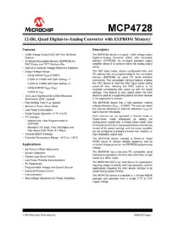
2 SECTION : COMPARATORS (cont.). INPUT CIRCUITRY SECTION : Analog MULTIPLIERS SECTION : RMS TO DC CONVERTERS SECTION : PROGRAMMABLE GAIN AMPLIFIERS SECTION : AUDIO AMPLIFIERS AMPLIFIERS VCAs (VOLTAGE CONTROLLED AMPLIFIERS) LINE DRIVERS AND RECEIVERS AUDIO LINE RECEIVERS AUDIO LINE DRIVERS CLASS-D POWER AMPLIFIERS SECTION : AUTO-ZERO AMPLIFIERS CHOPPER AMPLIFIERS AUTO-ZERO AMPLIFERS IMPROVE ON CHOPPERS IMPLEMENTATION OPERATION DESCRIPTION REFERENCES other linear circuits . BUFFER AMPLIFIERS. CHAPTER 2: other linear circuits . SECTION : BUFFER AMPLIFIERS. In the early days of high speed circuits , simple emitter followers were often used as high speed buffers. The term buffer was generally accepted to mean a unity-gain, open-loop amplifier. With the availability of matching PNP transistors, a simple emitter follower can be improved, as shown below in Figure This complementary circuit offers first- order cancellation of dc offset voltage, and can achieve bandwidths greater than 100 MHz.
3 Typical offset voltages without trimming are usually less than 50 mV, even with unmatched discrete transistors. +VS. +VS. VIN. R2. VS. VIN VOUT VOUT. +VS. VS R1. VS. (A) HOS-100 (B) LH0033. Figure : Early Open-Loop Hybrid Buffer Amplifiers: (A) HOS-100 Bipolar, (B) LH0033 FET Input If high input impedance is required, a dual FET can be used as an input stage ahead of a complementary emitter follower, as shown in Figure This form of the buffer circuit was implemented by both National Semiconductor Corporation as the LH0033, and by Analog Devices as the ADLH0033. circuits such as these achieved bandwidths of about 100 MHz at fairly respectable levels of harmonic distortion, typically better than 60 dBc. However, they suffered from dc and ac nonlinearities when driving loads less than 500 . BASIC linear DESIGN. One of the first totally monolithic implementations of these functions was the Precision Monolithics, Inc. BUF03 shown below in Figure (see Reference 1).
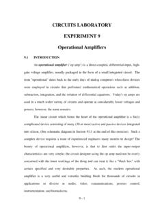
4 PMI is now a division of Analog Devices . This open-loop IC buffer achieved a bandwidth of about 50 MHz for a 2 V peak-to-peak signal. The BUF03 circuit is interesting because it demonstrates techniques that eliminated the requirement for the slow, bandwidth-limited vertical PNP transistors associated with most IC processes available at the time of the design (approximately 1979). +VS. J2 Q7. Q9. Q1. Q6 VOUT. J5. VIN. J1 230 A. Q5. J6 Q8. 230 A. Q11. Q10. VS. Figure : BUF03 Monolithic Open-Loop Buffer 1979 Vintage One of the problems with all the open-loop buffers discussed thus far is that although high bandwidths can be achieved, the Devices discussed don't take advantage of negative feedback. Distortion and dc performance suffer considerably when open-loop buffers are loaded with typical video impedance levels of 50 , 75 , or 100 . The solution is to use a properly compensated wide bandwidth op amp in a unity-gain follower configuration.
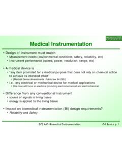
5 In the early days of monolithic op amps, process limitations prevented this, so the open-loop approach provided a popular interim solution. Practically all unity-gain-stable voltage or current feedback op amps can be used in a simple follower configuration. Usually, however, the general-purpose op amps are compensated to operate over a wide range of gains and feedback conditions. Therefore, bandwidth suffers somewhat at low gains, especially in the unity-gain noninverting mode, and additional external compensation is usually required. other linear circuits . BUFFER AMPLIFIERS. +.. Figure : Simple Unity-Gain Monolithic Buffers A practical solution is to compensate the op amp for the desired closed-loop gain, while including the gain setting resistors on-chip, as shown in Figure Note that this form of op amp, internally configured as a buffer, may typically have no feedback pin. Also, putting the resistors and compensation on-chip also serves to reduce parasitics.
6 There are a number of op amps optimized in this manner. Roy Gosser's AD9620 (see Reference 2) was probably the earliest monolithic implementation. The AD9620 was a 1990 product release, and achieved a bandwidth of 600 MHz using 5 V supplies. It was optimized for unity gain, and used the voltage feedback architecture. A newer design based on similar techniques is the AD9630, which achieves a 750 MHz bandwidth. +.. RF. CF. Figure : Frequency Compensated Buffer The BUF04 unity gain buffer (see Reference 3) was released in 1994 and achieves a bandwidth of 120 MHz. This device was optimized for large signals and operates on supplies from 5 V to 15 V. Because of the wide supply range, the BUF04 is useful not only as a standalone unity-gain buffer, but also within a feedback loop with a standard op amp, to boost output. Although the common definition of a buffer is unity gain device, sometimes the term is used for a circuit with a gain of 2.
7 Closed-loop buffers with a gain of 2 find wide applications as transmission line drivers, as shown below in Figure The internally configured fixed gain of the amplifier compensates for the loss incurred by the source and load termination. Impedances of 50 , 75 , and 100 are popular cable impedances. The AD8074/AD8075 500 MHz triple buffers are optimized for gains of 1 and 2, BASIC linear DESIGN. respectively. The dual AD8079A/AD8079B 260 MHz buffer is optimized for gains of 2. and , respectively. +. RS ZO.. RF RL. RS = RL = ZO. CF. RG AD8074 AD8075 AD8079A/B. Triple Triple Dual Voltage Feedback Voltage Feedback Voltage Feedback G=1 G=2 G = 2 / BW = 500 MHz BW = 500 MHz BW = 260 MHz VS = 5V VS = 5V VS = 5V. Figure : Fixed-Gain Video Transmission Line Drivers In implementing a high speed unity-gain buffer with a voltage feedback op amp, there will typically be no resistor required in the feedback loop, which considerably simplifies the circuit.
8 Note that this isn't a 100% hard-and-fast rule, however, so always check the device data sheet to be sure. A unity-gain buffer with a current feedback op amp will always require a feedback resistor, typically in the range of 500 to 1000 . So, be sure to use a value appropriate to not only the basic part, but also the specific power supplies in use. other linear circuits . GAIN BLOCKS. SECTION : GAIN BLOCKS. While the op amp allows gain to be set with external resistors, there are a group of circuits that are designed to operate at a fixed gain. These parts are typically RF. components. They also are typically designed to be operated in a 50 environment, with the inputs and outputs matched internally. Often the gain blocks are available in several gain settings. For example, the AD8354 RF gain block is a fixed-gain amplifier with single-ended input and output ports whose impedances are nominally equal to 50 over the frequency range 100 MHz to GHz.
9 Consequently, it can be directly inserted into a 50 system with no impedance matching circuitry required. The input and output impedances are sufficiently stable versus variations in temperature and supply voltage that no impedance matching compensation is required. Figure : AD8352 20 dB RF Gain Block Differential input and output gain blocks are also available. An example of a differential input, single-ended output device is the AD8129. See Figure AD8129/. AD8130. +IN 1 8 IN. VS 2 7 +VS. +. PD 3 6 OUT. REF 4 5 FB. Figure : AD8129/AD8130 Differential Input, Single-Ended Output Gain Block BASIC linear DESIGN. Fully differential input and output Devices are also available, such as the AD8350. See Figure IN+ 1 8 IN . ENBL 2 + 7 GND. VCC 3 6 GND. OUT+ 4 5 OUT . AD8350. Figure : AD8350 Differential In/Differential Out Gain Block other linear circuits . INSTRUMENTATION AMPLIFIERS. SECTION : INSTRUMENTATION AMPS. The instrumentation amp is primarily used to amplify small differential voltages in the presence of (typically) larger common-mode voltages.
10 In-Amp Definitions An in-amp is a precision closed-loop gain block. It has a pair of differential input terminals, and a single-ended output that works with respect to a reference or common terminal, as shown in Figure The input impedances are balanced and high in value, 9. typically 10 . Again, unlike an op amp, an in-amp uses an internal feedback resistor network, plus one (usually) gain set resistance, RG. Also unlike an op amp is the fact that the internal resistance network and RG are isolated from the signal input terminals. In amp gain can also be preset via an internal RG by pin selection, (again isolated from the signal inputs). Typical in amp gains range from 1 to 1000. The in-amp develops an output voltage which is referenced to a pin usually designated REFERENCE, or VREF. In many applications, this pin is connected to circuit ground, but it can be connected to other voltages, as long as they lie within the rated compliance range of the in-amp.