Transcription of HDMI/DVI Buffer with Equalization Data Sheet …
1 HDMI/DVI Buffer with Equalization data Sheet ad8195 Rev. B Information furnished by analog devices is believed to be accurate and reliable. However, n o responsibility is assumed by analog devices for its use, nor for any infringements of patents or other rights of third parties that may result from its use. Specifications subject to change without notice. No license is granted by implication or otherwise under any patent or patent rights of analog devices . Trademarks and registered trademarks are the property of their respective owners. One Technology Way, Box 9106, Norwood, MA 02062-9106, Tel: Fax: 2008 2012 analog devices , Inc. All rights reserved. FEATURES 1 input, 1 output HDMI/DVI link Enables HDMI front panel input 4 TMDS channels per link Supports 250 Mbps to Gbps data rates Supports 25 MHz to 225 MHz pixel clocks Equalized inputs for operation with long HDMI cables (20 m at Gbps) Preemphasized outputs Fully buffered unidirectional inputs/outputs 50 on-chip terminations Low added jitter Transmitter disable feature Reduces power dissipation Disables input termination 3 auxiliary buffered channels per link Bidirectional buffered DDC lines (SDA and SCL) Bidirectional buffered CEC line with integrated pull-up resistors (27 k ) Independently powered from 5 V of HDMI input connector Logic level translation ( V, 5 V) Input/output capacitance isolation Standards compatible.
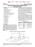
2 HDMI, DVI, HDCP, DDC, CEC 40-lead LFCSP_VQ package (6 mm 6 mm) APPLICATIONS Front panel Buffer for advanced television (HDTV) sets GENERAL DESCRIPTION The ad8195 is an HDMI/DVI Buffer featuring equalized TMDS inputs and preemphasized TMDS outputs, ideal for systems with long cable runs. The ad8195 includes bidirectional buffering for the DDC bus and bidirectional buffering with integrated pull-up resistors for the CEC bus. The DDC and CEC buffers are powered independently of the TMDS buffers so that DDC/ CEC functionality can be maintained when the system is powered off. The ad8195 meets all the requirements for sink tests as defined in Section 8 of the HDMI Compliance Test The ad8195 is specified to operate over the 40 C to +85 C temperature range. FUNCTIONAL BLOCK DIAGRAM IP[3:0]IN[3:0]VTTIOP[3:0]AMUXVCCAVEEVTTO AVCCON[3:0]VREF_INVREF_OUT+ + EQBUFFERPECONTROLLOGIC444224 HIGH SPEEDBUFFEREDLOW SPEEDBUFFEREDPE_ENTX_ENCOMPPARALLELBIDIR ECTIONALAD8195 SCL_INSDA_INSCL_OUTSDA_OUTCEC_INCEC_OUT0 7049-001 Figure 1.
3 TYPICAL APPLICATION 07049-002 MEDIA CENTERSET-TOP BOXDVD PLAYERHDTV SET4:1 HDMISWITCHAD8195 HDMIRECEIVERFRONT PANELCONNECTORBACK PANELCONNECTORSGAMECONSOLE Figure 2. Typical ad8195 Application for HDTV Sets PRODUCT HIGHLIGHTS 1. Enables a fully HDMI compliant front panel input. 2. Supports data rates of up to Gbps, enabling 1080p deep color ( 12-bit color) HDMI formats and greater than UXGA (1600 1200) DVI resolutions. 3. Input cable equalizer enables use of long cables; more than 20 meters (24 AWG) at data rates of up to Gbps. 4. Auxiliary Buffer isolates and buffers the DDC bus and CEC line for a single chip, fully HDMI compliant solution. 5. Auxiliary Buffer is powered independently from the TMDS link so that DDC/CEC functionality can be maintained when the system is powered off. ad8195 data Sheet Rev. B | Page 2 of 20 TABLE OF CONTENTS Features.
4 1 Applications .. 1 General Description .. 1 Functional Block Diagram .. 1 Ty pi cal Application .. 1 Product Highlights .. 1 Revision History .. 2 Specifications .. 3 TMDS Performance Specifications .. 3 Auxiliary Channel Performance 4 Power Supply and Control Logic Specifications .. 4 Absolute Maximum Ratings .. 5 Thermal Resistance .. 5 Maximum Power Dissipation .. 5 ESD Caution .. 5 Pin Configuration and Function Descriptions ..6 Typical Performance Characteristics ..8 Theory of Operation .. 13 Input Channels .. 13 Output Channels .. 13 Preemphasis .. 14 Auxiliary Lines .. 14 Applications Information .. 15 Front Panel Buffer for Advanced TV .. 15 Cable Lengths and Equalization .. 16 TMDS Output Rise/Fall Times .. 16 PCB Layout Guidelines .. 16 Outline Dimensions .. 19 Ordering Guide .. 19 REVISION HISTORY 8/12 R e v. A to R e v.
5 B Changed data Rate = 3 Gbps to data Rate = Gbps .. Throughout Changes to Features Section, General Description Section, and Product Highlights Section .. 1 Changes to Table 1 .. 3 Changes to specifications statements in Typical Performance Characteristics Section .. 8 Changes to Figure 19 .. 11 Changes to Theory of Operation Section and to Input Channels Section .. 13 Changes to Output Channels Section .. 13 Changes to Preemphasis Section .. 14 Changes to Cable Lengths and Equalization Section and PCB Layout Guidelines Section .. 16 Added Unused DDC/CEC Buffers Section .. 18 8/11 R e v. 0 t o R e v. A Changed data Rate = Gbps to data Rate = Gbps .. Throughout Changes to Features Section, General Description Section, and Product Highlights Section .. 1 Changes to Table 1 .. 3 Changes to Table 3 .. 4 Changes to Figure 5 Caption and Figure 7 Caption.
6 8 Added Figure 6 and Figure 8; Renumbered Sequentially .. 8 Moved Figure 9 and Figure 11 .. 9 Changes to Figure 9 Caption and Figure 11 Caption .. 9 Added Figure 10 and Figure 12 .. 9 Moved Figure 14 and Figure 16 .. 10 Changes to Figure 14 Caption and Figure 16 Caption .. 10 Added Figure 15 and Figure 17 .. 10 Changes to Figure 18, Figure 19, and Figure 21 .. 11 Changes to Input Channels Section .. 13 Changes to Output Channels Section .. 13 Changes to Preemphasis Section .. 14 Changes to Cable Lengths and Equalization Section, TMDS Output Rise/Fall Times Section, and PCB Layout Guidelines Section .. 16 Changes to Auxiliary Control Signals Section .. 18 8/08 Revision 0: Initial Version data Sheet ad8195 Rev. B | Page 3 of 20 SPECIFICATIONS TA = 27 C, AVCC = V, VTTI = V, VTTO = V, AMUXVCC = 5 V, VREF_IN = 5 V, VREF_OUT = 5 V, AVEE = 0 V, differential input swing = 1000 mV, TMDS outputs terminated with external 50 resistors to V, unless otherwise noted.
7 TMDS PERFORMANCE SPECIFICATIONS Table 1. Parameter Test Conditions/Comments Min Typ Max Unit TMDS DYNAMIC PERFORMANCE Maximum data Rate (DR) per Channel NRZ Gbps Bit Error Rate (BER) PRBS 223 1 10 9 Added data Jitter DR Gbps, PRBS 27 1 31 ps p-p Added Clock Jitter 1 ps rms Differential Intrapair Skew At output 1 ps Differential Interpair Skew At output 30 ps TMDS Equalization PERFORMANCE Receiver1 Boost frequency = GHz 12 dB Transmitter2 Boost frequency = GHz 6 dB TMDS INPUT CHARACTERISTICS Input Voltage Swing Differential 150 1200 mV Input Common-Mode Voltage (VICM) AVCC 800 AVCC mV TMDS OUTPUT CHARACTERISTICS High Voltage Level Single-ended, high speed channel AVCC 200 AVCC + 10 mV Low Voltage Level Single-ended, high speed channel AVCC 600 AVCC 400 mV Rise/Fall Time (20% to 80%)
8 3 DR = Gbps 50 90 150 ps TMDS TERMINATION Input Termination Resistance Single-ended 50 Output Termination Resistance Single-ended 50 1 Output meets transmitter eye diagram as defined in the DVI Standard Revision and HDMI Standard. 2 Cable output meets receiver eye diagram mask as defined in the DVI Standard Revision and HDMI Standard. 3 Output rise/fall time measurement excludes external components, such as HDMI connector or external ESD protection diodes. See the Applications Information section for more information. ad8195 data Sheet Rev. B | Page 4 of 20 AUXILIARY CHANNEL PERFORMANCE SPECIFICATIONS Table 2. Parameter Test Conditions/Comments Min Typ Max Unit DDC CHANNELS Input Capacitance, CAUX DC bias = V, ac voltage = V p-p, f = 100 kHz 10 15 pF Input Low Voltage, VIL V Input High Voltage, VIH VREF1 VREF1 V Output Low Voltage, VOL IOL = 5 mA V Output High Voltage, VOH VREF1 V Rise Time 10% to 90%, no load 140 ns Fall Time 90% to 10%, CLOAD = 400 pF 100 200 ns Leakage Input voltage = V 10 A CEC CHANNEL Input Capacitance, CAUX DC bias = V, ac voltage = V p-p, f = 100 kHz, 2 k pull-up resistor from CEC_OUT to V 5 25 pF Input Low Voltage, VIL V Input High Voltage, VIH V Output Low Voltage, VOL V Output High Voltage, VOH V Rise Time 10% to 90%, CLOAD = 1500 pF, RPULL-UP = 27 k.
9 Or CLOAD = 7200 pF, RPULL-UP = 3 k 50 100 s Fall Time 90% to 10%, CLOAD = 1500pF, RPULL-UP = 27 k ; or CLOAD = 7200 pF, RPULL-UP = 3 k 5 10 s Pull-Up Resistance 27 k Leakage Off leakage test conditions2 A 1 VREF is the voltage at the reference pin (VREF_IN for SCL_IN and SDA_IN, or VREF_OUT for SCL_OUT and SDA_OUT); nominally V. 2 Off leakage test conditions are described in the HDMI Compliance Test Specification Section 8, Test ID 8-14: Remove power (mains) from DUT. Connect CEC line to V via 27 k 5% resistor with ammeter in series. Measure CEC line leakage. POWER SUPPLY AND CONTROL LOGIC SPECIFICATIONS Table 3. Parameter Test Conditions/Comments Min Typ Max Unit POWER SUPPLY AVCC Operating range ( V 10%) 3 V AMUXVCC Operating range (5 V 10%) 5 V VREF_IN, VREF_OUT 3 V QUIESCENT CURRENT AVCC Output disabled 20 40 mA Output enabled, no preemphasis (0 dB) 32 50 mA Output enabled, maximum preemphasis (6 dB) 66 80 mA VTTI Input termination on 40 54 mA VTTO Output termination on, no preemphasis 40 50 mA Output termination on, maximum preemphasis 80 100 mA VREF_IN 120 200 A VREF_OUT 120 200 A AMUXVCC 10 20 mA POWER DISSIPATION Output disabled 116 254 mW Output enabled, no preemphasis (0 dB) 180 663 mW Output enabled, maximum preemphasis (6 dB) 736 1047 mW PARALLEL CONTROL INTERFACE TX_EN, PE_EN Input High Voltage, VIH V Input Low Voltage, VIL V data Sheet ad8195 Rev.
10 B | Page 5 of 20 ABSOLUTE MAXIMUM RATINGS Table 4. Parameter Rating AVCC to AVEE V VTTI AVCC + V VTTO AVCC + V AMUXVCC V VREF_IN V VREF_OUT V Internal Power Dissipation W High Speed Input Voltage AVCC V < VIN < AVCC + V High Speed Differential Input Voltage V Parallel Control Input Voltage AVEE V < VIN < AVCC + V Storage Temperature Range 65 C to +125 C Operating Temperature Range 40 C to +85 C Junction Temperature 150 C ESD, Human Body Model Input Pins Only 5 kV All Other Pins 3 kV Stresses above those listed under Absolute Maximum Ratings may cause permanent damage to the device. This is a stress rating only; functional operation of the device at these or any other conditions above those indicated in the operational section of this specification is not implied. Exposure to absolute maximum rating conditions for extended periods may affect device reliability.