Transcription of Interleaved Inverting Charge Pump with Negative LDO ...
1 Interleaved Inverting Charge Pump with Negative LDO Regulator Data Sheet ADP5600 Rev. A Document Feedback Information furnished by Analog Devices is believed to be accurate and reliable. However, no responsibility is assumed by Analog Devices for its use, nor for any infringements of patents or other rights of third parties that may result from its use. Specifications subject to change without notice. No license is granted by implication or otherwise under any patent or patent rights of Analog Devices. Trademarks and registered trademarks are the property of their respective owners. One Technology Way, Box 9106, Norwood, MA 02062-9106, Tel: 2020 2021 Analog Devices, Inc.
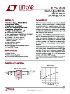
2 All rights reserved. Technical Support FEATURES Input voltage: V to 16 V Maximum output current: 100 mA Integrated power MOSFETs Four LDO selectable output voltage options V, V, V, 5 V Adjustable output voltage range: V to VIN + V Programmable Charge pump switching frequency range 100 kHz to 1 MHz Frequency synchronization via SYNC pin Precision enable and power good Internal soft start Output short-circuit and overload protection Shorted Charge pump fly capacitor protection Integrated LDO output discharge resistor 16-lead, 4 mm 4 mm LFCSP APPLICATIONS Powering the Negative rail on bipolar/split supply ADC/DAC/AMP/mux applications TYPICAL APPLICATIONS CIRCUITS CC21 FCIN10 FENSYNCFREQSEL1RT110k SEL2 PGOODGNDRPGOOD10k C1+ADP5600C1 CC11 FC2+C2 CPOUTCPOUTVCPOUT = ~ 12 VLDO_OUTFBONOFFVINVIN = 12 VCCPOUT10 FVLDO_OUT = F21096-001 Figure 1.
3 Fixed Output Voltage, VLDO_OUT = V CC21 FCIN10 FENSYNCFREQSEL1RT110k SEL2 PGOODGNDRPGOOD10k R2100k C1+ADP5600C1 CC11 FC2+C2 CPOUTCPOUTVCPOUT = ~ 12 VLDO_OUTFBONOFFVINVIN = 12 VCCPOUT10 FVADJ = F21096-002 Figure 2. Adjustable Output Voltage, VADJ = V GENERAL DESCRIPTION The ADP5600 is an Interleaved Charge pump inverter with an integrated, Negative , low dropout (LDO) linear regulator. The Interleaved Charge pump inverter exhibits reduced output voltage ripple and reflected input current noise over conventional inductive or conventional capacitive based solutions. The integrated LDO provides a rail with good regulation at sufficient power supply rejection ratio (PSRR).
4 The ADP5600 Charge pump operates via resistor programming or external clock synchronization at switching frequency range of 100 kHz to 1 MHz. Operating at a higher switching frequency allows the use of small input, output, and fly capacitors. To combine the high switching frequency with internal field effect transistors (FETs), compensation, and soft start gives a best-in-class total solution size for Negative rail generation. The ADP5600 also features comprehensive fault protection for robust applications. These protections include overload protection, shorted fly capacitor protection, undervoltage lockout (UVLO), and thermal shutdown. For easy sequencing, the ADP5600 has a power-good pin.
5 The integrated LDO of the ADP5600 uses an advanced proprie-tary architecture to provide high power supply rejection. It also achieves decent line and load transient response with only a small F ceramic output capacitor. The output can be configured via the SEL1 and SEL2 pins to one of four fixed output voltages and is adjustable from V to VIN + V via an external feedback divider. ADP5600 Data Sheet Rev. A | Page 2 of 25 TABLE OF CONTENTS Features .. 1 Applications .. 1 Typical Applications CircuitS .. 1 General Description .. 1 Revision History .. 2 Specifications .. 3 Charge Pump Regulator Specifications .. 4 LDO Regulator Specifications.
6 4 Recommended Input and Output Capacitor Specifications .. 5 Absolute Maximum Ratings .. 6 Thermal Resistance .. 6 ESD 6 Pin Configuration and Function Descriptions .. 7 Typical Performance Characteristics .. 8 Theory of Operation .. 14 Inverting Charge Pump Operation .. 14 Interleaved Inverting Charge Pump Operation .. 15 Charge Pump Output Resistance .. 16 Negative LDO Regulator .. 16 Startup and Soft Start .. 16 Precision Enable/Shutdown .. 17 Oscillator .. 17 Synchronization .. 17 Current-Limit and Output Short-Circuit Protection (SCP) 18 Power Good .. 18 Undervoltage Lockout (UVLO) .. 18 Thermal Considerations .. 19 Applications Information.
7 20 Capacitor Selection .. 20 Output Voltage Settings .. 20 noise Reduction .. 21 Changing the Oscillator Source On-the-Fly .. 21 Design Example .. 23 Setting the Switching Frequency of the Charge Pump .. 23 Selecting the Charge Pump Flying Capacitor .. 23 Setting the Output Voltage of the LDO Regulator .. 23 Determining the Minimum VIN Voltage .. 23 Circuit Board Layout Recommendations .. 24 Outline Dimensions .. 25 Ordering Guide .. 25 REVISION HISTORY 4/ 2021 Rev. 0 to Rev. A Change to Note 1, Table 6 .. 6 Changes to Typical Performance Characteristics Section .. 8 Change to Figure 40 .. 14 Changes to Interleaved Inverting Charge Pump Operation Section.
8 15 Changes to noise Reduction Section .. 21 Changes to Setting the Output Voltage of the LDO Regulator Section .. 23 Changes to Figure 65 Caption .. 25 7/ 2020 Revision 0: Initial Version Data Sheet ADP5600 Rev. A | Page 3 of 25 SPECIFICATIONS VIN = VEN = V or |VLDO_OUT V| whichever is higher to 16 V, VLDO_OUT = V, CIN = CCPOUT = 10 F, C1 = C2 = 1 F, CLDO_OUT = F , ILDO_OUT = 10 mA, fOSC = 500 kHz, TJ = 40oC to +125 C for minimum/maximum specifications unless otherwise noted. VIN = VEN = 12 V, TA = 25 C for typical specifications, unless otherwise noted. Table 1. Parameters Symbol Min Typ Max Unit Test Conditions/Comments POWER SUPPLY REQUIREMENTS Input Voltage VIN 16 V Active Switching Current ISW 4 mA VIN = 5 V, fOSC = 100 kHz 5 mA VIN = 5 V, fOSC = 500 kHz mA VIN = 5 V, fOSC = 1 MHz mA VIN = 16 V, fOSC = 500 kHz Shutdown Current ISHDN A EN = GND, VIN =16 V VIN Undervoltage Lockout Threshold UVLORISING V VIN rising UVLOFALLING V VIN falling UVLOHYS 90 mV VIN falling SEL1, SEL2 PULL-UP CURRENT ISEL 5 A VSELx = V THERMAL SHUTDOWN Threshold TSDRISING 150 C Hysteresis TSDHYS 20 C EN EN Shutdown Threshold (High to Low)
9 ENSD2 V Threshold to enter shutdown EN Rising Threshold, Precision ENTH V Precision threshold EN Input Hysteresis, Precision ENHYS 70 mV EN noise Filter Time ENFILT_LO-HI s EN low to high noise filter EN Leakage Current A VIN = VEN = 16 V OSCILLATOR (FREQ) Oscillator Frequency Range fOSC MHz Frequency range of the resistor programmable internal oscillator FREQ Resistor Range RT 0 530 k FREQ = GND Frequency Range fOSC_GND MHz RT = 0 FREQ Voltage VFREQ 1 V Buffered output SYNC Synchronization Range fSYNC MHz fOSC = fSYNC/2 SYNC Minimum Pulse Width tSYNC_MIN_ON 100 ns SYNC Minimum Off Time tSYNC_MIN_OFF 150 ns SYNC Input High Voltage VIH_SYNC V SYNC Input Low Voltage VIL_SYNC V SYNC Leakage Current ISYNC_LKG 100 nA VSYNC = V POWER-GOOD OUTPUT Rising Threshold PGTH 91 93 95 % Nominal VLDO_OUT Hysteresis PGHYS 3 % Power-Good Rising
10 Deglitch Time tPG 16 1/fOSC Power-Good Leakage Current IPG_LKG 5 100 nA VPG =16 V Power-Good Output Low Voltage VOL 130 209 mV IPG = 1 mA ADP5600 Data Sheet Rev. A | Page 4 of 25 Charge PUMP REGULATOR SPECIFICATIONS Table 2. Parameters Symbol Min Typ Max Unit Test Conditions/Comments Charge PUMP OUTPUT IMPEDANCE ROUT ICPOUT = 50 mA ON RESISTANCES VIN to Cx+ PFET Switch RCPHx x = Inverting Charge Pump 1 or Charge Pump 2 Cx to GND PFET Switch RCPGx Cx+ to GND NFET Switch RFNGx Cx to CPOUT NFET Switch RFNOx