Transcription of IRF1407 - Infineon Technologies
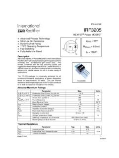
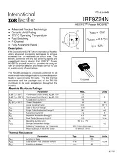
1 @ TC = 25 CContinuous Drain Current, VGS @ 10V130 ID @ TC = 100 CContinuous Drain Current, VGS @ 10V92 AIDMP ulsed Drain Current 520PD @TC = 25 CPower Dissipation330 WLinear Derating CVGSGate-to-Source Voltage 20 VEASS ingle Pulse avalanche Energy 390mJIARA valanche Current See , 12b, 15, 16 AEARR epetitive avalanche Energy mJdv/dtPeak Diode Recovery dv/dt Junction and-55 to + 175 TSTGS torage Temperature RangeSoldering Temperature, for 10 seconds300 ( from case ) CMounting Torque, 6-32 or M3 screw10 lbf in ( m)HEXFET Power MOSFETS pecifically designed for Automotive applications, this Stripe Planardesign of HEXFET Power MOSFETs utilizes the lastest processingtechniques to achieve extremely low on-resistance per silicon features of this HEXFET power MOSFET are a 175 C junctionoperating temperature, fast switching speed and improved repetitiveavalanche rating.
2 These benefits combine to make this design an extremelyefficient and reliable device for use in Automotive applications and a widevariety of other Maximum RatingsVDSS = 75 VRDS(on) = ID = 130A Description10/11 Advanced Process Technology Ultra Low On-Resistance Dynamic dv/dt Rating 175 C Operating Temperature Fast Switching Repetitive avalanche Allowed up to TjmaxBenefitsTypical Applications Integrated Starter Alternator 42 Volts Automotive Electrical SystemsAUTOMOTIVE MOSFETTO-220 ABPD - JCJunction-to-Case CSCase-to-Sink, Flat, Greased C/WR JAJunction-to-Ambient 62 Thermal Typ. Max. Units ConditionsV(BR)DSSD rain-to-Source Breakdown Voltage75 VVGS = 0V, ID = 250 A V(BR)DSS/ TJBreakdown Voltage Temp.
3 Coefficient V/ C Reference to 25 C, ID = 1mARDS(on)Static Drain-to-Source On-Resistance VGS = 10V, ID = 78A VGS(th)Gate Threshold = 10V, ID = 250 AgfsForward Transconductance74 SVDS = 25V, ID = 78A 20 AVDS = 75V, VGS = 0V 250 VDS = 60V, VGS = 0V, TJ = 150 CGate-to-Source Forward Leakage 200 VGS = 20 VGate-to-Source Reverse Leakage -200nAVGS = -20 VQgTotal Gate Charge 160250ID = 78 AQgsGate-to-Source Charge 3552nCVDS = 60 VQgdGate-to-Drain ("Miller") Charge 5481 VGS = 10V td(on)Turn-On Delay Time 11 VDD = 38 VtrRise Time 150 ID = 78 Atd(off)Turn-Off Delay Time 150 RG = tfFall Time 140 VGS = 10V Between lead, 6mm ( )from packageand center of die contactCissInput Capacitance 5600 VGS = 0 VCossOutput Capacitance 890 pFVDS = 25 VCrssReverse Transfer Capacitance 190 = , See Fig.
4 5 CossOutput Capacitance 5800 VGS = 0V, VDS = , = Capacitance 560 VGS = 0V, VDS = 60V, = Output Capacitance 1100 VGS = 0V, VDS = 0V to 60 VnHElectrical Characteristics @ TJ = 25 C (unless otherwise specified)LDInternal Drain InductanceLSInternal Source Inductance Leakage CurrentSDG ParameterMin. Units ConditionsISContinuous Source CurrentMOSFET symbol(Body Diode) showing theISMP ulsed Source Currentintegral reverse(Body Diode) p-n junction Forward Voltage = 25 C, IS = 78A, VGS = 0V trrReverse Recovery Time 110170nsTJ = 25 C, IF = 78 AQrrReverse RecoveryCharge 390590nCdi/dt = 100A/ s tonForward Turn-On TimeIntrinsic turn-on time is negligible (turn-on is dominated by LS+LD)Source-Drain Ratings and Characteristics130 520A Repetitive rating; pulse width limited by max.
5 Junction temperature. (See fig. 11). Starting TJ = 25 C, L = RG = 25 , IAS = 78A. (See Figure 12). ISD 78A, di/dt 320A/ s, VDD V(BR)DSS, TJ 175 C Pulse width 400 s; duty cycle 2%.Notes: Coss eff. is a fixed capacitance that gives the same charging time as Coss while VDS is rising from 0 to 80% VDSS . Calculated continuous current based on maximum allowable junction temperature. Package limitation current is 75A. Limited by TJmax , see , 12b, 15, 16 for typical repetitive avalanche 4. Normalized On-Resistancevs. TemperatureFig 2. Typical Output CharacteristicsFig 1. Typical Output CharacteristicsFig 3. Typical Transfer , Drain-to-Source Voltage (V)1101001000ID, Drain-to-Source Current (A) s PULSE WIDTHTj = 25 C VGSTOP 15V 10V , Drain-to-Source Voltage (V)1101001000ID, Drain-to-Source Current (A) s PULSE WIDTHTj = 175 C VGSTOP 15V 10V , Gate-to-Source Voltage (V) , Drain-to-Source Current ( )TJ = 25 CTJ = 175 CVDS = 15V20 s PULSE , Junction Temperature( C)R , Drain-to-Source On Resistance(Normalized)JDS(on)
6 V=I= 8. Maximum Safe Operating AreaFig 6. Typical Gate Charge VoltageFig 5. Typical Capacitance VoltageFig 7. Typical Source-Drain DiodeForward Voltage110100 VDS, Drain-to-Source Voltage (V)100100010000100000C, Capacitance(pF)CossCrssCissVGS = 0V, f = 1 MHZCiss = Cgs + Cgd, Cds SHORTEDCrss = Cgd Coss = Cds + Cgd0408012016020003691215Q , Total Gate Charge (nC)V , Gate-to-Source Voltage (V)GGS I=D78A V= 15 VDSV= 37 VDSV= , Source-toDrain Voltage (V) , Reverse Drain Current (A)TJ = 25 CTJ = 175 CVGS = 0V1101001000 VDS , Drain-toSource Voltage (V)110100100010000ID, Drain-to-Source Current (A)Tc = 25 CTj = 175 CSingle Pulse1msec10msecOPERATION IN THIS AREA LIMITED BY RDS(on)100 9. Maximum Drain Current TemperatureVDS90%10%VGStd(on)trtd(off)tf VDSP ulse Width 1 sDuty Factor % +-VDDFig 10a.
7 Switching Time Test CircuitFig 10b. Switching Time WaveformsFig 11. Maximum Effective Transient Thermal Impedance, Junction-to-Case255075100125150175020406 080100120140T , Case Temperature( C)I , Drain Current (A) CD LIMITED BY 1 Notes:1. Duty factor D =t / t2. Peak T=Px Z+ T12 JDMthJCC PttDM12t , Rectangular Pulse Duration (sec)Thermal Response(Z ) = SINGLE PULSE(THERMAL RESPONSE) F50K .2 F12 VCurrent RegulatorSame Type as Sampling Resistors+-10 VFig 13b. Gate Charge Test CircuitFig 13a. Basic Gate Charge WaveformFig 12c. Maximum avalanche Energyvs. Drain CurrentFig 12b. Unclamped Inductive WaveformsFig 12a. Unclamped Inductive Test CircuittpV(BR) +-VDDDRIVERA15V20 VFig 14. Threshold Voltage vs.
8 Temperature25507510012515017501302603905 20650 Starting T , Junction Temperature( C)E , Single Pulse avalanche Energy (mJ)JAS IDTOPBOTTOM32A 55A 78A -75-50-250255075100125150175200TJ , Temperature ( C ) (th) Gate threshold Voltage (V)ID = 250 15. Typical avalanche Current 16. Maximum avalanche Energyvs. TemperatureNotes on Repetitive avalanche Curves , Figures 15, 16:(For further info, see AN-1005 at )1. avalanche failures assumption: Purely a thermal phenomenon and failure occurs at a temperature far in excess of Tjmax. This is validated for every part Safe operation in avalanche is allowed as long asTjmax is not Equation below based on circuit and waveforms shown in Figures 12a, PD (ave) = Average power dissipation per single avalanche BV = Rated breakdown voltage ( factor accounts for voltage increase during avalanche ).
9 6. Iav = Allowable avalanche T = Allowable rise in junction temperature, not to exceed Tjmax (assumed as 25 C in Figure 15, 16). tav = Average time in avalanche . D = Duty cycle in avalanche = tav f ZthJC(D, tav) = Transient thermal resistance, see figure 11)PD (ave) = 1/2 ( BV Iav) = T/ ZthJCIav = 2 T/ [ BV Zth]EAS (AR) = PD (ave) (sec)1101001000 avalanche Current (A) Cycle = Single avalanche Current vs avalanche pulsewidth, tav assuming Tj = 25 C due to avalanche TJ , Junction Temperature ( C)0100200300400 EAR , avalanche Energy (mJ)TOP Single Pulse BOTTOM 10% Duty CycleID = Diode Recovery dv/dt Test Recoverydv/dtRipple 5%Body Diode Forward DropRe-AppliedVoltageReverseRecoveryCurr entBody Diode ForwardCurrentVGS=10 VVDDISDD river Gate VDSW aveformInductor CurentD = P.
10 W .Period+-+++--- RGVDD dv/dt controlled by RG ISD controlled by Duty Factor "D" - Device Under *Circuit Layout Considerations Low Stray Inductance Ground Plane Low Leakage Inductance Current Transformer * Reverse Polarity of for P-ChannelVGS[ ][ ]** VGS = for Logic Level and 3V Drive Devices[ ] **Fig 17. For N-channel HEXFET power ASSIGNMENTS 1 - G A T E 2 - D R A IN 3 - S O U R C E 4 - D R A IN- B (.052) (.048) (.022) (.018) (.115) (.104) (.185) (.165) (.037) (.027) (.160) (.140) (.045) M (.255) (.240) (.149) (.139)- A (.415) (.405) (.113) (.103) (.600) (.584) (.555) (.530) (.055) (.045) (.100) 6 ( .014 ) M B A M41 2 3 NOTES: 1 DIMENSIONING & TOLER ANCING PER ANS I , 1982.