Transcription of Lecture 12: MOS Transistor Models
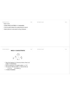
1 Department of EECSU niversity of California, BerkeleyEECS 105 Fall 2003, Lecture 12 Lecture 12: MOS Transistor ModelsProf. NiknejadDepartment of EECSU niversity of California, BerkeleyEECS 105 Fall 2003, Lecture 12 Prof. A. NiknejadLecture Outline MOS Transistors ( ) I-V curve (Square-Law Model) Small Signal Model (Linear Model)Department of EECSU niversity of California, BerkeleyEECS 105 Fall 2003, Lecture 12 Prof. A. NiknejadObserved Behavior: ID-VGS Current zero for negative gate voltage Current in Transistor is very low until the gate voltage crosses the threshold voltage of device (same threshold voltage as MOS capacitor) Current increases rapidly at first and then it finally reaches a point where it simply increases linearlyGSVDSITVGSVDSIDSVD epartment of EECSU niversity of California, BerkeleyEECS 105 Fall 2003, Lecture 12 Prof.
2 A. NiknejadObserved Behavior: ID-VDS For low values of drain voltage, the device is like a resistor As the voltage is increases, the resistance behaves non-linearly and the rate of increase of current slows Eventually the current stops growing and remains essentially constant (current source)DSV/DSIk constant currentresistor regionnon-linear resistor region2 GSVV=3 GSVV=4 GSVV=GSVDSIDSVD epartment of EECSU niversity of California, BerkeleyEECS 105 Fall 2003, Lecture 12 Prof. A. Niknejad Linear Region Current If the gate is biased above threshold, the surface is inverted This inverted region forms a channel that connects the drain and gate If a drain voltage is applied positive, electrons will flow from source to drainp-typen+n+p+Inversion layer channel GSTnVV>100mVDSV GDSNMOSxyDepartment of EECSU niversity of California, BerkeleyEECS 105 Fall 2003, Lecture 12 Prof.
3 A. NiknejadMOSFET: Variable Resistor Notice that in the linear region, the current is proportional to the voltage Can define a voltage-dependent resistor This is a nice variable resistor, electronically tunable!()DSnoxGSTnDSWICVVVL = 1()()DSeqGSDSnoxGSTnVLLRRVICVVWW === Department of EECSU niversity of California, BerkeleyEECS 105 Fall 2003, Lecture 12 Prof. A. NiknejadFinding ID= f(VGS, VDS) Approximate inversion charge QN(y): drain is higher than the source less charge at drain end of channelDepartment of EECSU niversity of California, BerkeleyEECS 105 Fall 2003, Lecture 12 Prof. A.
4 NiknejadInversion Charge at Source/Drain)()0()(LyQyQyQNNN=+= )()0(TnGSoxNVVCyQ ====)(LyQN)(TnGDoxVVC DSGSGDVV =Department of EECSU niversity of California, BerkeleyEECS 105 Fall 2003, Lecture 12 Prof. A. NiknejadAverage Inversion Charge Charge at drain end is lower since field is lower Simple approximation: In reality we should integrate the total charge minus the bulk depletion charge across the channel()()()2oxGS ToxGD TNCVVCV VQy + Source EndDrain End()()()2oxGSToxGSSDTNCVVCVVVQy + (22 )()()22oxGSTox SDDSNoxGSTCV V CVVQyCV V = Department of EECSU niversity of California, BerkeleyEECS 105 Fall 2003, Lecture 12 Prof.
5 A. NiknejadDrift Velocity and Drain Current Long-channel assumption: use mobility to find v()()(/ )nDSnnVvyEyV yL = =Substituting:()2 DSDSDNoxGSTVVIWvQW CVVL = ()2 DSDoxGSTDSVWICVVVL Inverted ParabolasDepartment of EECSU niversity of California, BerkeleyEECS 105 Fall 2003, Lecture 12 Prof. A. NiknejadSquare-Law CharacteristicsBoundary: what is ID,SAT?TRIODE REGIONSATURATION REGIOND epartment of EECSU niversity of California, BerkeleyEECS 105 Fall 2003, Lecture 12 Prof. A. NiknejadThe Saturation RegionWhen VDS> VGS VTn, there isn t any inversioncharge at the drain.
6 According to our simplistic modelWhy do curvesflatten out?Department of EECSU niversity of California, BerkeleyEECS 105 Fall 2003, Lecture 12 Prof. A. NiknejadSquare-Law Current in SaturationCurrent stays at maximum (where VDS= VGS VTn= VDS,SAT)Measurement: IDincreases slightly with increasing VDSmodel with linear fudge factor ()2 DSDoxGSTDSVWICVVVL = ,()()2 GSTDS satoxGSTGSTVVWICVV VVL = 2,()2oxDS satGSTCWIVVL = 2,()(1)2oxDS satGSTDSCWIVVVL = +Department of EECSU niversity of California, BerkeleyEECS 105 Fall 2003, Lecture 12 Prof. A. NiknejadPinching the MOS Transistors When VDS> VDS,sat, the channel is pinched off at drain end (hence the name pinch-off region ) Drain mobile charge goes to zero (region is depleted), the remaining elecricfield is dropped across this high-field depletion region As the drain voltage is increases further, the pinch off point moves back towards source Channel Length Modulation.
7 The effective channel length is thus reduced higher IDSp-typen+n+p+Pinch-Off PointGSTnVV>DSVGDSNMOSD epletion RegionGSTnVV Department of EECSU niversity of California, BerkeleyEECS 105 Fall 2003, Lecture 12 Prof. A. NiknejadLinear MOSFET ModelChannel (inversion) charge: neglect reduction at drainVelocity saturation defines VDS,SAT =EsatL = constant-vsat/ nDrain current:)],()[(,TnGSoxsatNSATDVVCvWWvQI = =|Esat| = 104V/cm, L= m VDS,SAT= V!)1)((,DSnTnGSoxsatSATDVVVWCvI + =Department of EECSU niversity of California, BerkeleyEECS 105 Fall 2003, Lecture 12 Prof. A. NiknejadWhy Find an Incremental Model?
8 Signals of interest in analog ICs are often of the form:Direct substitution into iD= f(vGS, vDS) is tedious AND doesn t include charge-storage effects ..pretty rough approximation()()GSGS gsvt V vt=+Fixed Bias PointSmall SignalDepartment of EECSU niversity of California, BerkeleyEECS 105 Fall 2003, Lecture 12 Prof. A. NiknejadWhich Operating Region?3 VGSV=3 VDSV=TRIODESATOFFD epartment of EECSU niversity of California, BerkeleyEECS 105 Fall 2003, Lecture 12 Prof. A. NiknejadChanging One Variable at a TimeAssumption: VDS> VDS,SAT= VGS VTn(square law)GSV/DSIk3 VDSV=1 VTV=Square LawSaturationRegionLinear TriodeRegionSlope of Tangent: Incremental current increaseDepartment of EECSU niversity of California, BerkeleyEECS 105 Fall 2003, Lecture 12 Prof.
9 A. NiknejadThe Transconductance gmDefined as the change in drain current due to a change in the gate-sourcevoltage, with everything else constant,,()(1)GSDSGSDSDDmoxGSTDSGSGSVVV ViiWgCVVVvvL === + 2,()(1)2oxDS satGSTDSCWIVVVL = +()moxGSTWgCVVL = 0 22 DSmoxoxDSoxIWWgCCIWLLCL ==2()DSmGSTIgVV= Gate BiasDrain Current BiasDrain Current Bias and Gate BiasDepartment of EECSU niversity of California, BerkeleyEECS 105 Fall 2003, Lecture 12 Prof. A. NiknejadOutput Resistance roDefined as the inverse of the change in drain current dueto a change in the drain-sourcevoltage, with everythingelse constantNon-Zero SlopeDSV DSI Department of EECSU niversity of California, BerkeleyEECS 105 Fall 2003, Lecture 12 Prof.
10 A. NiknejadEvaluating ro1,GSDSDoDSVVirv = 2()(1)2oxDGSTDSCWiVVVL = +021()2oxGSTrCWVVL = 01 DSrI Department of EECSU niversity of California, BerkeleyEECS 105 Fall 2003, Lecture 12 Prof. A. NiknejadTotal Small Signal Current()DSDS dsitI i=+DSDS dsgsdsgsdsiiivvvv =+ 1dsm gsdsoigvvr=+TransconductanceConductanceD epartment of EECSU niversity of California, BerkeleyEECS 105 Fall 2003, Lecture 12 Prof. A. NiknejadPutting Together a Circuit Model1dsmgsdsoigvvr=+Department of EECSU niversity of California, BerkeleyEECS 105 Fall 2003, Lecture 12 Prof. A. NiknejadRole of the Substrate PotentialNeed not be the source potential, but VB< VSEffect: changes threshold voltage, which changes the drain current.