Example: quiz answers
Lecture 13 - MIT
• Following logic gates: must add capacitance of each gate of every transistor the output is connected to. • Interconnect wires that connects output to input of following logic gates • Own drain-to-body capacitances CL =CG +Cwire+CDBn+CDBp V DD C L V IN V OUT V IN V DD V DD V DD 1 2 3 W L W L p1 W L p2 W L n2 W L p3 W L n3 n1 (a) + − (b)
Tags:
Information
Domain:
Source:
Link to this page:
Documents from same domain
Chapter 21 Rigid Body Dynamics: Rotation and …
web.mit.eduChapter 21 Rigid Body Dynamics: Rotation and ... patience to the establishment of the laws of rotation of the solid ... general treatment of mechanics, ...
Wireless Communications and Networks
web.mit.edu4 MIT Physical layer •The physical layer plays a very important role in wireless network because it has severe limitation on transmissions Uplink with respect to downlink
The Aleph - MIT
web.mit.eduThe Aleph by Jorge Luis Borges O God! ... He read me many other stanzas, each of which also won his own approval and elicited his lengthy explications.
Finite Element Method
web.mit.eduRobert Cook, Finite Element Modeling For Stress Analysis, John Wiley & Sons, 1995 Introduction to Finite Element Method, http://210.17.155.47 (in Korean)
Finite Element Analysis
web.mit.eduFinite Element Analysis David Roylance Department of Materials Science and Engineering Massachusetts Institute of Technology Cambridge, MA 02139 February 28, …

TECHNICAL & SERVICE MANUAL - MIT
web.mit.eduwhen wiring electrical shock can cause severe personal injury or death. only a qualified, experienced electrician should attempt to wire this system.
5.33 Lecture Notes: Introduction To Polymer …
web.mit.edu5.33 Lecture Notes: Introduction To Polymer Chemistry Polymer: A large molecule (macromolecule) built up by repetitive bonding (covalent) of smaller molecules (monomers) • Generally not a well defined structure, or molecular weight.
UNDERSTANDING, FINDING, & ELIMINATING …
web.mit.edua Senior Member of the Institute of Electrical and Electronic Engineers. CEDIA EST016 UNDERSTANDING, ... GROUNDING, AC POWER, AND SAFETY ...
PRESENTED AT THE 2004 AMERICAN CONTROL …
web.mit.eduPRESENTED AT THE 2004 AMERICAN CONTROL CONFERENCE 1 Internal and External Op-Amp Compensation: A Control-Centric Tutorial ... circuit operational …
Frank and Lillian Gilbreth and the Manufacture and ...
web.mit.eduFrank and Lillian Gilbreth and the Manufacture ... time study, despite its ... publicizing micro-motion study as an advance over time study and as an
Related documents

VLSI Layout Examples - Obviously Awesome
bjpcjp.github.ioChapter 15 VLSI Layout Examples 413 Standard-Cell Examples Standard cells are layouts of logic elements including gates, flip-flops, and ALU functions that are available in a cell library for use in the design of a chip. Custom design refers to the design of cells or standard cells using MOSFETs at the lowest level.
Chapter 1 Introduction to CMOS Circuit Design
www.ee.ncu.edu.twSwitch: MOSFET MOSFETs are basic electronic devices used to direct and control logic signals in IC design MOSFET: Metal-Oxide-Semiconductor Field-Effect Transistor N-type MOS (NMOS) and P-type MOS (PMOS) Voltage-controlled switches A MOSFET has four terminals: gate, source, drain, and substrate (body) Complementary MOS (CMOS)
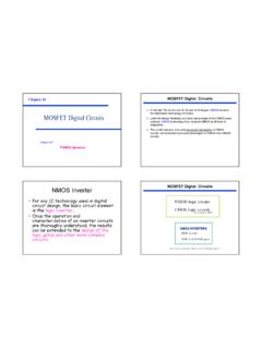
Chapter 16.1 NMOS Inverter - cankaya.edu.tr
ece424.cankaya.edu.trChap.3 ÆÆ NMOS Inverter • For any IC technology used in digital circuit design, the basic circuit element is the logic inverter. • Once the operation and characterization of an inverter circuits are thoroughly understood, the results can be extended to the design of the logic gates and other more complex circuits.

In Praise of - University of California, San Diego
neurophysics.ucsd.eduabout the authors Anant Agarwal is Professor of Electrical Engineering and Computer Science at the Massachusetts Institute of Technology. He joined the faculty in 1988, teaching courses in circuits and electronics, VLSI, digital logic and computer architecture.
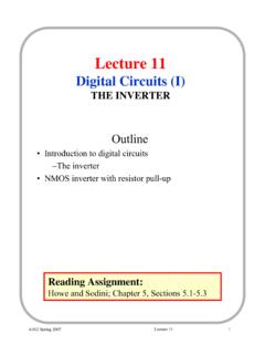
Lecture 11 - Massachusetts Institute of Technology
web.mit.edu6.012 Spring 2007 Lecture 11 7 Simplifications for hand calculations: Logic levels and noise margins • Assume VOL ≈VMIN and VOH ≈VMAX • Trace tangent of transfer function at VM – Slope = small signal voltage gain (Av) at VM •VIL ≈intersection of tangent with VOUT = VMAX •VIH ≈intersection of tangent with VOUT = VMIN It is hard to compute points in transfer …