Transcription of LM358 - Diodes Incorporated
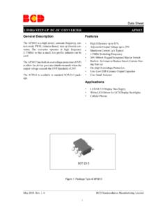
1 LM358 LOW POWER DUAL OPERATIONAL AMPLIFIERS LM358 Document number: DS35167 Rev. 2 - 2 1 of 14 February 2011 Diodes Incorporated NEW PRODUCT Description The LM358 series consists of two independent, high gain,internally frequency compensated operational amplifierswhich were designed specifically to operate from a singlepower supply over a wide range of voltages. Operation fromsplit power supplies is also possible and the low powersupply current drain is independent of the magnitude of thepower supply voltage . Application areas include transducer amplifiers, dc gainblocks and all the conventional op amp circuits which nowcan be more easily implemented in single power supplysystems.
2 For example, the LM358 series can be directlyoperated from the standard +5V power supply voltage whichis used in digital systems and will easily provide the requiredinterface electronics without requiring an additional 15 Vpower supply. Features Internally frequency compensated for unity gain Large dc voltage gain: 100 dB Very low supply current drain (500 A); essentially independent of supply voltage Wide bandwidth (unity gain): 1 MHz (temperature compensated) Input common-mode voltage range includes ground Differential input voltage range equal to the power supply voltage Low input offset voltage : 2mV Wide power supply range: o Single supply: 3V to 32V o Dual supplies: to 16V Large output voltage swing.
3 0V to V+ - SOP-8L packaging Green Molding Compound (No Br, Sb) Lead Free Finish/ RoHS Compliant (Note 1) Pin Assignments Applications Eliminates the need for dual supplies Compatible with all forms of logic Two internally compensated op amps Low power drain ideal for battery operation Allows direct sensing near GND VOUT can swing to GND Unique Characteristics In the linear mode the input common-mode voltage range includes ground and the output voltage can also swing to ground, whilst operating from only a single power supply voltage . The unity gain crossing frequency is temperature compensated. The input bias current is temperature compensated. Notes: 1.
4 EU Directive 2002/95/EC (RoHS). All applicable RoHS exemptions applied. Please visit our website at LM358 NON-INVERTING INPUT 2 INVERTING INPUT 2V+OUTPUT 2 SOP-8L(TOP VIEW)OUTPUT 1 NON-INVERTING INPUT 1 GNDINVERTING INPUT 143215678 LM358 LOW POWER DUAL OPERATIONAL AMPLIFIERS LM358 Document number: DS35167 Rev. 2 - 2 2 of 14 February 2011 Diodes Incorporated NEW PRODUCT Typical Single-Supply Circuit (V+= ) +-+VOR21MR110K+VIN**R no t ne ed ed d ue to t em peratu re inde pen de nt IINNon-Inverting DC Gain (0V Output)+-+VOR21MR110K+VIN**R no t ne ed ed d ue to t em peratu re inde pen de nt IINNon-Inverting DC Gain (0V Output)DC Summing Amplifier(VIN 'S>0 VDCand VO>0 VDC)+-R100 KR100 KR100 KR100 K+V1+V2+V3+V4R10 0KR1 00 KVOW here: VO=V1+V2-V3-V4(V1+V2) > (V3+V4) to kee p VO> 0 VDCDC Summing Amplifier(VIN 'S>0 VDCand VO>0 VDC)+-R100 KR100 KR100 KR100 K+V1+V2+V3+V4R10 0KR1 00 KVOW here.
5 VO=V1+V2-V3-V4(V1+V2) > (V3+V4) to kee p VO> 0 VDC+-VOV+R191 0KR2100 KR391 KRL+VINP ower AmplifierVO=0 VDC for VIN= 0 VDCAV=10+-VOV+R191 0KR2100 KR391 KRL+VINP ower AmplifierVO=0 VDC for VIN= 0 VDCAV=10VO(Volts)VIN(m V )GA IN= 1+=101(as shown)R2R1+5 VVO(Volts)VIN(m V )GA IN= 1+=101(as shown)R2R1+5V+-+-+-V+C23 30p F"BI-QUAD" RC Active Bandpass FilterR1100 KR2100KR3100KR410 MR547 0KR6100 KR8100 KR74 70KC133 0pFC310 F+VOVINfO= 1KH zQ = 50+-+-+-V+C23 30p F"BI-QUAD" RC Active Bandpass FilterR1100 KR2100KR3100KR410 MR547 0KR6100 KR8100 KR74 70KC133 0pFC310 F+VOVINfO= 1KH zQ = 50 LM358 LOW POWER DUAL OPERATIONAL AMPLIFIERS LM358 Document number: DS35167 Rev. 2 - 2 3 of 14 February 2011 Diodes Incorporated NEW PRODUCT Typical Single-Supply Circuit (Continued) (V+= ) +-1m AV+2VR12KI1 Fixed Current Sources+-2V+-R42KR32KR23KI2I1= I2+-1m AV+2VR12KI1 Fixed Current Sources+-2V+-R42KR32KR23KI2I1= I2-+R210 0R1* MonitorVO=1V(IL) A*(In crea se R1 for ILsmall)VL<V+ -2V-+R210 0R1* MonitorVO=1V(IL) A*(In crea se R1 for ILsmall)
6 VL<V+ -2 VLED Driver82+-20 mALED Driver82+-20 mALamp DriverV+10 0 >20+-30 mA600 mALamp DriverV+10 0 >20+-30 mA600 mADriving TTL+-RL240 Driving TTL+-RL240 voltage Follower+-VO+VINVO = VINV oltage Follower+-VO+VINVO = VINP ulse Generator+-VO10 0KV+ 1 FR310 0KR410 0KR5100K+0 Pulse Generator+-VO10 0KV+ 1 FR310 0KR410 0KR5100K+0 Square wave OscillatorVO100KV+ FR21 00KR3100KR4100 K+0+-Square wave OscillatorVO100KV+ FR21 00KR3100KR4100 K+0+- LM358 LOW POWER DUAL OPERATIONAL AMPLIFIERS LM358 Document number: DS35167 Rev. 2 - 2 4 of 14 February 2011 Diodes Incorporated NEW PRODUCT Typical Single-Supply Circuit (Continued) (V+= ) +-+-+-+VINC1 F2N92 9**hi AT 1 00 FIB2 IBIBIBZIN(POLYCARBONATE ORPOL YETHYLEN E)HIGH ZINLOW ZOUTVOZOUTAUX AM PIN PUT CURRENTCOMPENSATIONLow Drift Peak Detector+-+-+-+VINC1 F2N92 9**hi AT 1 00 FIB2 IBIBIBZIN(POLYCARBONATE ORPOL YETHYLEN E)HIGH ZINLOW ZOUTVOZOUTAUX AM PIN PUT CURRENTCOMPENSATIONLow Drift Peak DetectorPulse Generator+-VO30KV+ 1R3100KR4100KR5100K+0IN914R2150K FPulse Generator+-VO30KV+ 1R3100KR4100KR5100K+0IN914R2150K FHigh Compliance Current Sink-++VINRL10 IOIO= amp / volt VIN(increase REfor IOsm al l)
7 High Compliance Current Sink-++VINRL10 IOIO= amp / volt VIN(increase REfor IOsm al l)+-+ 5 F+VC*OUTPUT1 voltage Controlled Oscillator (VCO)51K51 KR/ 250KR100 K10K10 0KV+/2 51 KOUTPUT2*WIDE CONTROL voltage RANGE: 0 VDC<VC<2 (V+ )+-+ 5 F+VC*OUTPUT1 voltage Controlled Oscillator (VCO)51K51 KR/ 250KR100 K10K10 0KV+/2 51 KOUTPUT2*WIDE CONTROL voltage RANGE: 0 VDC<VC<2 (V+ ) LM358 LOW POWER DUAL OPERATIONAL AMPLIFIERS LM358 Document number: DS35167 Rev. 2 - 2 5 of 14 February 2011 Diodes Incorporated NEW PRODUCT Typical Single-Supply Circuit (Continued) (V+= ) +-VOR210 M+VINC omparator with Hysteresis+VREFR110 K+-VOR210 M+VINC omparator with Hysteresis+VREFR110 KAC Coupled Inverting Amplifier+-R110 KVIN+CINRf10KR2100 KR3100KC110?
8 F+ VppAV= (As shown, AV=10 )RfR1V+AC Coupled Inverting Amplifier+-R110 KVIN+CINRf10KR2100 KR3100KC110?F+ VppAV= (As shown, AV=10 )RfR1V++-VOR41M+VCMG round Referencing a DifferentialInput SignalVRR11MR21MR31MR+-VO=VR+-VOR41M+VCM G round Referencing a DifferentialInput SignalVRR11MR21MR31MR+-VO=VRAC Coupled Non-Inverting Amplifier+-VIN+ F+ VppR21MR31MC210? FR41 00KR51 00KV+AV=1+R2R1AV=11(As Sh own)AC Coupled Non-Inverting Amplifier+-VIN+ F+ VppR21MR31MC210? FR41 00KR51 00KV+AV=1+R2R1AV=11(As Sh own)+-VOR410 0 KVINDC Coupled Low-Pass RC Active ? 0 KVOfO0fO = 1 KHzQ = 1AV=2+-VOR410 0 KVINDC Coupled Low-Pass RC Active ? 0 KVOfO0fO = 1 KHzQ = 1AV=2 High Input Z, DC Differential Amplifier+-VO+-R310 0KR4100 KR2100KR1100 K+V1+V2R1R2R4R3Fo r =(CMRR depends on thisresistor ratio match)VO= (1+ )(V2-V1)R4R3As Sh own: VO= 2(V2-V1)High Input Z, DC Differential Amplifier+-VO+-R310 0KR4100 KR2100KR1100 K+V1+V2R1R2R4R3Fo r =(CMRR depends on thisresistor ratio match)VO= (1+ )(V2-V1)R4R3As Sh own: VO= 2(V2-V1) LM358 LOW POWER DUAL OPERATIONAL AMPLIFIERS LM358 Document number: DS35167 Rev.
9 2 - 2 6 of 14 February 2011 Diodes Incorporated NEW PRODUCT Typical Single-Supply Circuit (Continued) (V+= ) Bandpass Active Filter+-R1390 ?F+VOV++ 1?FC310? FR262 0KR3680R4390 KR539KR61 20KR710 0KR81 00 KfO= KH zQ = 25 Bandpass Active Filter+-R1390 ?F+VOV++ 1?FC310? FR262 0KR3680R4390 KR539KR61 20KR710 0KR81 00 KfO= KH zQ = 25+-+-+-+V1+V2R12 KGAIN ADJUSTR210 0KR3100 KR4100 KR510 0KR6100 KR7100 KVOAs Sh own: VO= 101(V2-V1)VO=( 1 + )(V2-V1)2R2R1I f R1 = R5 & R3 = R 4 = R6 = R7 (C MRR d epe nds o n m atch)High Input Z Adjustable-GainDC Instrumentation Amplifier+-+-+-+V1+V2R12 KGAIN ADJUSTR210 0KR3100 KR4100 KR510 0KR6100 KR7100 KVOAs Sh own: VO= 101(V2-V1)VO=( 1 + )(V2-V1)2R2R1I f R1 = R5 & R3 = R 4 = R6 = R7 (C MRR d epe nds o n m atch)High Input Z Adjustable-GainDC Instrumentation Amplifier+-+-+VIN+ M2R3MA UX AM PINPU T CURRENTCOMPENSATIONU sing Symmetrical Amplifiers to ReduceInput Current (General Concept)2N92 9**h i ?
10 AT 50 nA+-+-+VIN+ M2R3MA UX AM PINPU T CURRENTCOMPENSATIONU sing Symmetrical Amplifiers to ReduceInput Current (General Concept)2N92 9**h i ? AT 50 nA LM358 LOW POWER DUAL OPERATIONAL AMPLIFIERS LM358 Document number: DS35167 Rev. 2 - 2 7 of 14 February 2011 Diodes Incorporated NEW PRODUCT Functional Block Diagram INVERTING INPUT 1 GNDNON-INVERTING INPUT 1 OUTPUT 2 OUTPUT 1 INVERTING INPUT 2 NON-INVERTING INPUT 212345678AB+-+-V+ Pin Descriptions Pin Name Pin # Description OUTPUT 1 1 Channel 1 Output INVERTING INPUT 1 2 Channel 1 Inverting Input NON-INVERTING INPUT 1 3 Channel 1 Non-inverting Input GND 4 Ground NON-INVERTING INPUT 2 5 Channel 2 Non-inverting Input INVERTING INPUT 2 6 Channel 2 Inverting Input OUTPUT 2 7
