Search results with tag "Offset voltage"
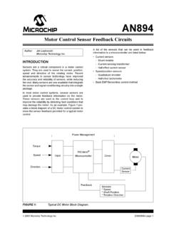
Motor Control Sensor Feedback Circuits
ww1.microchip.com• Increasing R SENSE increases the V SENSE voltage, which makes the voltage offset (VOS) and input bias current offset (IOS) amplifier errors less significant. • A large R SENSE value causes a voltage loss and a reduction in the power efficiency due to the I 2 x R loss of the resistor. Regr a•A l SENSE value will cause a voltage offset to
a Ultralow Offset Voltage Operational Amplifiers OP07
www.mit.edu–4– REV. A OP07–SPECIFICATIONS OP07E ELECTRICAL CHARACTERISTICS Parameter Symbol Conditions Min Typ Max Unit INPUT CHARACTERISTICS Input Offset Voltage1 V OS 45 130 µV Voltage Drift without External Trim2 TCV OS 0.3 1.3 µV/°C Voltage Drift with External Trim3 TCV OSN R P = 20 kΩ 0.3 1.3 µV/°C Input Offset Current I
LMV321 - Single, Dual, Quad Low-Voltage, Rail-to-Rail ...
www.onsemi.comLMV324 are CMOS single, dual, and quad low voltage operational amplifiers with rail−to−rail output swing. These amplifiers are a cost−effective solution for applications where low power consumption ... Input Offset Voltage VIO TA = TLow to THigh (Note 6) 1.7 9 mV Input Offset Voltage Average Drift TCVIO TA = TLow to THigh (Note 6) 5 V/°C

Precision, Ultralow Noise, RRIO, Zero-Drift Op Amp Data ...
www.analog.comADA4528-1/ADA4528-2 are ultralow noise, zero-drift operational amplifiers featuring rail-to-rail input and output swing. With an offset voltage of 2.5 μV, offset voltage drift of 0.015 μV/°C, and typical noise of 97 nV p-p (0.1 Hz to 10 Hz, A V = +100), the ADA4528-1/ADA4528-2 …

MC33272A - Operational Amplifiers, Single Supply, High ...
www.onsemi.comLow Input Offset Voltage The MC33272/74 series of monolithic operational amplifiers are quality fabricated with innovative Bipolar design concepts. This dual and quad operational amplifier series incorporates Bipolar inputs along with a patented Zip−R−Trim element for input offset voltage reduction.
Next Generation OP07 Ultralow Offset Voltage Operational ...
www.analog.comNext Generation OP07 Ultralow Offset Voltage Operational Amplifier Data Sheet OP77 Rev. G Document Feedback Information furnished by Analog Devices is believed to be accurate and reliable.

Ultra-Low Noise, Precision Operational Amplifiers ...
www.ti.comOPA27, OPA37 5 SBOS135C www.ti.com TYPICAL CHARACTERISTICS At TA = +25°C, ±VCC = ±15VDC, unless otherwise noted. INPUT OFFSET VOLTAGE WARM-UP DRIFT Time From Power Turn-On (min) 0 +10 +5 0 –5 –10 Offset Voltage Change

Ultraprecision Operational Amplifier
www.analog.comany operational amplifier currently available. Offset voltage of the OP177 is only 25 μV maximum at room temperature. The ultralow V. OS. of the OP177 combines with the exceptional offset voltage drift (TCV. OS) of 0.3 μV/°C maximum to eliminate the need for external V. OS . adjustment and increases system accuracy over temperature. The . OP177
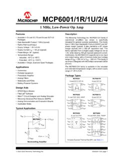
MCP6001/1R/1U/2/4 - 1 MHz, Low-Power Op Amp
ww1.microchip.comMay 14, 2019 · Input Offset Input Offset Voltage V OS-4.5 — +4.5 mV VCM = VSS (Note 1) Input Offset Drift with Temperature VOS/ TA —±2.0 — µV/°CTA= -40°C to +125°C, VCM = VSS Power Supply Rejection Ratio PSRR — 86 — dB V CM = VSS Input Bias Current and Impedance Input Bias Current: IB — ±1.0 — pA Industrial Temperature IB —19 — pATA ...
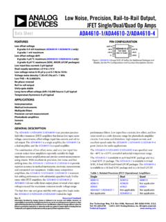
Low Noise, Precision, Rail-to-Rail Output, JFET Single ...
www.analog.comfield effect transistor (JFET) amplifiers that feature low input noise voltage, current noise, offset voltage, input bias current, and rail -to-rail output. The ADA4610-1 is a single amplifier , the ADA4610-2 is a dual amplifier, and the ADA4610-4 is a quad amplifier. The combination of low offset, noise, and very low input bias

Precision, Low Cost, High Speed BiFET Dual Op Amp Data ...
www.analog.comand 100% testing guarantee a low input offset voltage (3 mV maximum, J grade). Input offset voltage is specified in the warmed-up condition. 3. Together with precision dc performance, the AD712 offers excellent dynamic response. It settles to ±0.01% in 1 μs and has a minimum slew rate of 16 V/μs. Thus, this device is
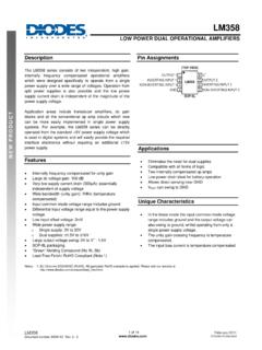
LM358 - Diodes Incorporated
www.diodes.com• Low input offset voltage: 2mV • Wide power supply range: o Single supply: 3V to 32V o Dual supplies: ±1.5V to ±16V • Large output voltage swing: 0V to V+ - 1.5V • SOP-8L packaging • “Green” Molding Compound (No Br, Sb) • Lead Free Finish/ RoHS Compliant (Note 1) Pin Assignments ...
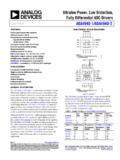
Ultralow Power, Low Distortion, Fully Differential ADC ...
www.analog.com0.35 mV maximum offset voltage Balanced outputs Settling time to 0.1%: 34 ns Rail-to-rail output: −V S + 0.1 V to +V S − 0.1 V Adjustable output common-mode voltage Flexible power supplies: 3 V to 7 V (LFCSP) Disable pin to reduce power consumption ADA4940-1 is available in LFCSP and SOIC packages APPLICATIONS Low power PulSAR®/SAR ADC drivers
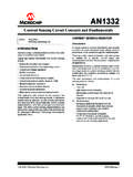
Current Sensing Circuit Concepts and Fundamentals
ww1.microchip.comHowever, the voltage drop across the sensing resistor may become low enough to be comparable to the input offset voltage of subsequent analog conditioning circuit, which would compromise the measurement accuracy. In addition, the current sensing resistor’s inherent inductance must be low, if the measured current has a large high-frequency ...

LT3042 - 20V, 200mA, Ultralow Noise, Ultrahigh PSRR RF ...
www.analog.com20V, 200mA, Ultralow Noise, ... Designed as a precision current reference followed by a high performance voltage buffer, the LT3042 can be easily paralleled to further reduce noise, increase output current and spread heat on the PCB. ... Output Offset Voltage VOS (VOUT – VSET)
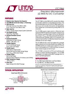
LTC1966 - Precision Micropower ΔΣ RMS-to-DC Converter
www.analog.comVIOS Input Offset Voltage (Notes 6, 7, 10) l 0.02 0.8 1.0 mV mV Accuracy vs Crest Factor (CF) CF = 4 60Hz Fundamental, 200mVRMS (Note 11) l –1 2 mV CF = 5 60Hz Fundamental, 200mVRMS (Note 11) l –20 30 mV Input Characteristics IVR Input Voltage Range (Note 14) l VSS VDD V ZIN Input Impedance Average, Differential (Note 12) Average, Common ...
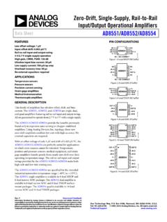
Zero-Drift, Single-Supply, Rail-to-Rail Input/Output ...
www.analog.comInput/Output Operational Amplifiers Data Sheet AD8551/AD8552/AD8554 ... Low offset voltage: 1 μV Input offset drift: 0.005 μV/°C . Rail-to-rail input and output swing . 5 V/2.7 V single-supply operation . High gain, CMRR, PSRR: 130 dB . Ultralow input bias current: 20 p A .

LM741-MIL Operational Amplifier datasheet
www.ti.comInput offset voltage adjustment range TA = 25°C, VS = ±20 V ±15 mV Input offset current TA = 25°C 20 200 nA 85 500 Input bias current ... The LM741-MIL device is a general-purpose operational amplifier which features improved performance over industry standards such as the LM709. It is intended for a wide range of analog applications.
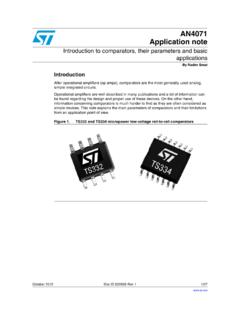
Introduction to comparators, their parameters and basic ...
www.st.comAN4071 Comparator parameters Doc ID 022939 Rev 1 5/27 2 Comparator parameters Comparator classification by major parameters Propagation delay Current consumption Output stage type (open collector/drain or push-pull) Input offset voltage, hysteresis Output current capability Rise and fall time Input common mode voltage range. Besides major parameters, …
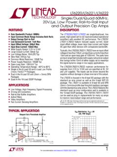
LT6220/LT6221/LT6222 - Single/Dual/Quad 60MHz, 20V/µs, …
www.analog.comn Low Quiescent Current: 1mA Max n Input Offset Voltage: 350µV Max n Input Bias Current: 150nA Max n Wide Supply Range: 2.2V to 12.6V n Large Output Current: 50mA Typ n Low Voltage Noise: 10nV√Hz Typ n Slew Rate: 20V/µs Typ n Common Mode Rejection: 102dB Typ n Power Supply Rejection: 105dB Typ n Open-Loop Gain: 100V/mV Typ

AD797 (Rev. K) - Analog Devices
www.analog.comThe AD797 is a very low noise, low distortion operational amplifier ideal for use as a preamplifier. The low noise of 0.9 nV/√Hz and ... Offset Voltage Drift ±5 V, ±15 V 0.2 1.0 0.2 0.6 μV/°C INPUT BIAS CURRENT ±5 V, ±15 V 0.25 1.5 0.25 0.9 μA T MIN to T MAX 0.5 3.0 ...
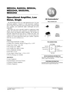
NE5534 - Operational Amplifier, Low Noise, Single
www.onsemi.comOperational Amplifier, Low Noise, Single The NE/SA/SE5534/5534A are single high-performance low noise operational amplifiers. Compared to other operational amplifiers, ... Offset Voltage Adjustment Circuit Figure 15. Closed-Loop Frequency Response 5534 5534 CC (nV Hz) (nV Hz) CAL OSC POWER SUPPLY CAL +VCC-VCC METER +40dB 10k 100 TEST BOARD GND ...

LM339 - Single Supply Quad Comparators
www.onsemi.comLM339, LM339E, LM239, LM2901, LM2901E, LM2901V, NCV2901, MC3302 www.onsemi.com 5 Figure 4. Normalized Input Offset Voltage Figure 5. Input Bias Current
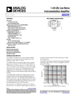
1 nV/√Hz Low Noise Instrumentation Amplifier Data Sheet …
www.analog.comInstrumentation Amplifier Data Sheet AD8429 ... 50 μV maximum input offset voltage 0.02% maximum gain accuracy (G = 1) Excellent ac specifications ... The AD8429 is an ultralow noise, instrumentation amplifier designed for measuring extremely small signals over a wide
Similar queries
Voltage, Voltage offset, Offset, Offset voltage, INPUT, Input Offset, Quad Low, Quad low voltage, Ultralow, Data, ADA4528, Operational, Quad, Analog Devices, Ultra-Low, Operational Amplifiers, Operational amplifier, OP177, MCP6001/1R/1U/2/4, 1 MHz, Low-Power Op Amp, Power, ADA4610, Low offset, ADA4940, Introduction to comparators, their parameters and basic, Low Voltage, Quad Comparators, Amplifier Data Sheet, Amplifier