Transcription of Next Generation OP07 Ultralow Offset Voltage Operational ...
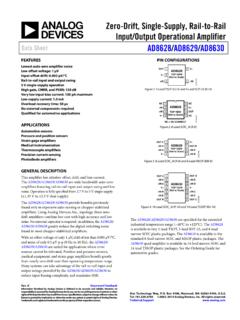
1 Next Generation OP07 Ultralow Offset Voltage Operational Amplifier Data Sheet OP77. FEATURES PIN CONNECTIONS. Outstanding gain linearity VOS TRIM 1 OP77 8 VOS TRIM. Ultrahigh gain, 5000 V/mV min IN 2 7 V+. Low VOS over temperature, 55 V max +IN 3 6 OUT. TCVOS, V/ C max V 4 TOP VIEW 5 NC. 00320-001. (Not to Scale). High PSRR, 3 V/V max NC = NO CONNECT. Low power consumption, 60 mW max Figure 1. 8-Pin Hermetic Available in die form CERDIP_Q-8 (Z Suffix). VOS TRIM. VOS TRIM 8 V+. 1 7. OP77. IN 2 6 OUT. 3 5. +IN 4 NC. 4V (CASE). TOP VIEW. 00320-002. (Not to Scale). NC = NO CONNECT. Figure 2. TO-99. (J Suffix). GENERAL DESCRIPTION. The OP77 has outstanding gain of 10,000,000 or more that is the need for VOS adjustment and increases system accuracy over maintained over the full 10 V output range. This gain-linearity temperature. eliminates incorrectable system nonlinearities common in A PSRR of 3 V/V (110 dB) and CMRR of V/V maximum previous monolithic op amps and provides superior performance virtually eliminate errors caused by power supply drifts and in high closed-loop gain applications.
2 Low initial VOS drift and common-mode signals. This combination of outstanding rapid stabilization time, combined with only 50 mW of power characteristics makes the OP77 ideally suited for high resolution consumption, are significant improvements over previous instrumentation and other tight error budget systems. designs. These characteristics, plus the TCVOS of V/ C. maximum and the low VOS of 25 V maximum, eliminates Rev. G Document Feedback Information furnished by analog devices is believed to be accurate and reliable. However, no responsibility is assumed by analog devices for its use, nor for any infringements of patents or other rights of third parties that may result from its use. Specifications subject to change without notice. No One Technology Way, Box 9106, Norwood, MA 02062-9106, license is granted by implication or otherwise under any patent or patent rights of analog devices . Tel: 2002 2015 analog devices , Inc. All rights reserved.
3 Trademarks and registered trademarks are the property of their respective owners. Technical Support OP77 Data Sheet TABLE OF CONTENTS. Features .. 1 Thermal Resistance ..6 Pin Connections .. 1 ESD General Description .. 1 Typical Performance Characteristics ..7 Revision History .. 2 Test Circuits .. 10 3 11 Electrical Specifications .. 3 Precision Current Sinks .. 12 Wafer Test Limits .. 4 Outline Dimensions .. 15 Typical Electrical Characteristics .. 5 Ordering Guide .. 16. Absolute Maximum 6 REVISION HISTORY. 10/15 Rev. F to Rev. G. Changes to Features Section and General Description 1. Changes to Note 1, Ordering 16. 3/15 Rev. E to Rev. F. Updated Outline Dimensions .. 15. Changes to Ordering Guide .. 16. 4/10 Rev. D to Rev. E. Removed Figure 33 and Two Subsequent Paragraphs .. 12. 6/09 Rev. C to Rev. D. Changes to Figure 1 and Figure 2 .. 1. Changes to Table 1 .. 3. Removed Endnote 1 and Endnote 2 in Table 3 .. 4. Changes to Figure 16.
4 9. Changes to Figure 31 and Figure 32 .. 12. Changes to Figure 38 .. 14. Moved Figure 39 .. 14. 10/02 Rev. B to Rev. C. Edits to Specifications .. 2. Figure 2 Caption Changed .. 10. Figure 3 Caption Changed .. 10. Edits to Figure 10 .. 11. Updated Outline Dimensions .. 15. 2/02 Rev. A to Rev. B. Remove 8-Lead SO PIN Connection Diagrams .. 1. Changes to Absolute Maximum 2. Remove OP77B column from Specifications .. 2. Remove OP77B column from Electrical Characteristics .. 3, 5. Remove OP77G column from Wafer Test 6. Remove OP77G column from Typical Electrical Characteristics .. 6. Rev. G | Page 2 of 16. Data Sheet OP77. SPECIFICATIONS. ELECTRICAL SPECIFICATIONS. @ VS = 15 V, TA = 25 C, unless otherwise noted. Table 1. OP77E OP77F. Parameter Symbol Conditions Min Typ Max Min Typ Max Unit INPUT Offset Voltage VOS 10 25 20 60 V. LONG-TERM STABILITY1 VOS/time V/Mo INPUT Offset CURRENT IOS nA. INPUT BIAS CURRENT IB + + + + nA. INPUT NOISE VOLTAGE2 enp-p Hz to 10 Hz Vp-p INPUT NOISE Voltage DENSITY en fO = 10 Hz nV/ Hz fO = 100 Hz2 fO = 1000 Hz INPUT NOISE CURRENT2 inp-p Hz to 10 Hz 14 30 15 35 pAp-p INPUT NOISE CURRENT DENSITY in fO = 10 Hz pA Hz fO = 100 Hz2 fO = 1000 Hz INPUT RESISTANCE.
5 Differential Mode3 RIN 26 45 45 M . Common Mode RINCM 200 200 G . INPUT Voltage RANGE IVR 13 14 13 14 V. COMMON-MODE REJECTION RATIO CMRR VCM = 13 V V/V. POWER SUPPLY REJECTION RATIO PSRR VS = 3 V to 18 V V/V. LARGE-SIGNAL Voltage GAIN AVO RL 2 k 5000 12,000 2000 6000 V/mV. VO = 10 V. OUTPUT Voltage SWING VO RL 10 k V. RL 2 k RL 1 k SLEW RATE2 SR RL 2 k V/ s CLOSED-LOOP BANDWIDTH2 BW AVCL + 1 MHz OPEN-LOOP OUTPUT RESISTANCE RO 60 60 . POWER CONSUMPTION Pd VS = 15 V, no load 50 60 50 60 mW. VS = 3 V, no load Offset ADJUSTMENT RANGE Rp = 20 kn 3 3 mV. 1. Long-term input Offset Voltage stability refers to the averaged trend line of VOS vs. time over extended periods after the first 30 days of operation. Excluding the initial hour of operation, changes in VOS during the first 30 operating days are typically V. 2. Sample tested. 3. Guaranteed by design. Rev. G | Page 3 of 16. OP77 Data Sheet @ VS = 15 V, 25 C TA +85 C for OP77FJ and OP77E/OP77F, unless otherwise noted.
6 Table 2. OP77E OP77F. Parameter Symbol Conditions Min Typ Max Min Typ Max Unit INPUT Offset Voltage VOS 10 45 20 100 V. AVERAGE INPUT Offset Voltage DRIFT1 TCVOS V/ C. INPUT Offset CURRENT IOS nA. AVERAGE INPUT Offset CURRENT DRIFT2 TCIOS 85 pA/ C. INPUT BIAS CURRENT IB + + + + nA. AVERAGE INPUT BIAS CURRENT DRIFT2 TCIB 8 40 15 60 pA/ C. INPUT Voltage RANGE IVR V. COMMON-MODE REJECTION RATIO CMRR VCM = 13 V pV/V. POWER SUPPLY REJECTION RATIO PSRR VS = 3 V to 18 V V/V. LARGE-SIGNAL Voltage GAIN AVO RL 2 k 2000 6000 1000 4000 V/mV. VO = 10 V. OUTPUT Voltage SWING VO RL 2 k 12 12 V. POWER CONSUMPTION Pd VS = 15 V, no load 60 75 60 75 mW. 1. OP77E: TCVOS is 100% tested on J and Z packages. 2. Guaranteed by end-point limits. WAFER TEST LIMITS. @ VS = 15 V, TA = 25 C, for OP77 NBC devices , unless otherwise noted. Table 3. Parameter Symbol Conditions OP77 NBC Limit Unit INPUT Offset Voltage VOS 40 V max INPUT Offset CURRENT IOS nA max INPUT BIAS CURRENT IB 2 nA max INPUT RESISTANCE.
7 Differential Mode RIN 26 M min INPUT Voltage RANGE IVR 13 V min COMMON-MODE REJECTION RATIO CMRR VCM = 13 V 1 V/V max POWER SUPPLY REJECTION RATIO PSRR VS = 3 V to 18 V 3 V/V max OUTPUT Voltage SWING VO RL = 10 k V min RL = 2 k RL = 1 k LARGE-SIGNAL Voltage GAIN AVO RL = 2 k 2000 V/mV min VO = 10 V. DIFFERENTIAL INPUT Voltage 30 V max POWER CONSUMPTION Pd VO = 0 V 60 mW max Rev. G | Page 4 of 16. Data Sheet OP77. TYPICAL ELECTRICAL CHARACTERISTICS. @ VS = 15 V, TA = 25 C, unless otherwise noted. Table 4. Parameter Symbol Conditions OP77 NBC Limit Unit AVERAGE INPUT Offset Voltage DRIFT TCVOS RS = 50 V/ C. NULLED INPUT Offset Voltage DRIFT TCVOSn RS = 50 , RP = 20 k V/ C. AVERAGE INPUT Offset CURRENT DRIFT TCIOS pA/ C. SLEW RATE SR RL 2 k V/ s BANDWIDTH BW AVCL + 1 MHz Rev. G | Page 5 of 16. OP77 Data Sheet ABSOLUTE MAXIMUM RATINGS. Table 5. Stresses at or above those listed under Absolute Maximum Ratings may cause permanent damage to the product.
8 This is a Parameter 1. Rating stress rating only; functional operation of the product at these Supply Voltage 22 V. or any other conditions above those indicated in the Operational Differential Input Voltage 30 V. section of this specification is not implied. Operation beyond Input Voltage2 22 V. the maximum operating conditions for extended periods may Output Short-Circuit Duration Indefinite affect product reliability. Storage Temperature Range 65 C to +150 C. Operating Temperature Range 25 C to +85 C THERMAL RESISTANCE. Junction Temperature (TJ) 65 C to +150 C. Table 6. Lead Temperature (Soldering, 60 sec) 300 C. Package Type JA1 JC Unit 1. Absolute Maximum Ratings apply to both dice and packaged parts, unless 8-Pin TO-99 H-08 (J Suffix) 150 18 C/W. otherwise noted. 2. For supply voltages less than 22 V, the absolute maximum input Voltage is 8-Lead Hermetic CERDIP Q-8 (Z Suffix) 148 16 C/W. equal to the supply Voltage . 1. JA is specified for worst-case mounting conditions, , JA is specified for a device in socket for the TO-99 and CERDIP packages.
9 ESD CAUTION. Rev. G | Page 6 of 16. Data Sheet OP77. TYPICAL PERFORMANCE CHARACTERISTICS. 2 30. VS = 15V. J, Z PACKAGES. TA = 25 C. + V/ C. 20. CHANGE IN Offset Voltage ( V). RL = 10k . (NULLED TO 0 V @ VOUT = 0V). 1. MEAN. INPUT Voltage ( V). 10. 0 0. 10. 1. 20. V/ C. 2 30. 00320-004. 00320-007. 10 5 0 5 10 55 35 15 5 25 45 65 85 105 125. OUTPUT Voltage (V) TEMPERATURE ( C). Figure 3. Gain Linearity (Input Voltage vs. Output Voltage ) Figure 6. Untrimmed Offset Voltage vs. Temperature 25 4. VS = 15V VS = 15V. CHANGE IN INPUT Offset Voltage ( V). 3 TA = 25 C. 20. 2. OPEN-LOOP GAIN (V/ V). 1. 15. 0. 10. 1. 2. 5. 3. 0 4. 00320-005. 00320-008. 55 35 15 5 25 45 65 85 105 125 0 TEMPERATURE ( C) TIME AFTER POWER SUPPLY TURN-ON (Minutes). Figure 4. Open-Loop Gain vs. Temperature Figure 7. Warm-Up Drift 16 30. TA = 25 C VS = 15V. RL = 2k . 25. ABSOLUTE CHANGE IN INPUT. DEVICE IMMERSED IN. 12. OPEN-LOOP GAIN (V/ V). 70 C OIL BATH (20 UNITS). Offset Voltage ( V).
10 20. 8 15. MAXIMUM. 10. 4. AVERAGE. 5. MIMIMUM. 0 0. 00320-006. 00320-009. 0 5 10 15 20 10 0 10 20 30 40 50 60 70. POWER SUPPLY Voltage (V) TIME (Seconds). Figure 5. Open-Loop Gain vs. Power Supply Voltage Figure 8. Offset Voltage Change Due to Thermal Shock Rev. G | Page 7 of 16. OP77 Data Sheet 100 130. VS = 15V TA = 25 C. TA = 25 C. 120. 80. CLOSED-LOOP GAIN (dB). 110. 60. PSRR (dB). 100. 40. 90. 20. 80. 0. 70. 20 60. 00320-013. 00320-010. 10 100 1k 10k 100k 1M 10M 1 10 100 1k 10k FREQUENCY (Hz) FREQUENCY (Hz). Figure 9. Closed-Loop Response for Various Gain Configurations Figure 12. PSRR vs. Frequency 160 0 4. VS = 15V VS = 15V. TA = 25 C. 140. INPUT BIAS CURRENT (nA). 120 45 3. OPEN-LOOP GAIN (dB). PHASE (Degrees). 100. 80 90 2. 60. 40 135 1. 20. 0 180 0. 00320-014. 00320-011. 1 10 100 1k 10k 100k 1M 75 50 25 0 25 50 75 100 125. FREQUENCY (Hz) TEMPERATURE ( C). Figure 10. Open-Loop Gain/Phase Response Figure 13. Input Bias Current vs.
