Transcription of Low Cost, High Speed, Rail-to-Rail Amplifiers Data Sheet ...
1 Low Cost, High Speed, Rail-to-Rail AmplifiersData Sheet AD8051/AD8052/AD8054 Rev. K Document Feedback Information furnished by Analog Devices is believed to be accurate and reliable. However, no responsibility is assumed by Analog Devices for its use, nor for any infringements of patents or other rights of third parties that may result from its use. Specifications subject to change without notice. No license is granted by implication or otherwise under any patent or patent rights of Analog Devices. Trademarks and registered trademarks are the property of their respective owners. One Technology Way, Box 9106, Norwood, MA 02062-9106, : 1997 2019 Analog Devices, Inc.
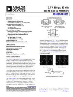
2 All rights reserved. Technical Support FEATURES High speed and fast settling on 5 V 110 MHz, 3 dB bandwidth (G = +1) (AD8051/AD8052) 150 MHz, 3 dB bandwidth (G = +1) (AD8054) 145 V/ s slew rate 50 ns settling time to Single-supply operation Output swings to within 25 mV of either rail input voltage range: V to +4 V; VS = 5 V Video specifications (G = +2) dB gain flatness: 20 MHz; RL = 150 Differential gain/phase: Low distortion 80 dBc total harmonic @ 1 MHz, RL = 100 Outstanding load drive capability Drives 45 mA, V from supply rails (AD8051/AD8052) Drives 50 pF capacitive load (G = +1) (AD8051/AD8052) Low power: mA/amplifier (AD8054) Low power: mA/amplifier (AD8051/AD8052) APPLICATIONS Active filters Analog-to-digital drivers Clock buffer Consumer video Professional cameras CCD imaging systems CD/DVD ROMs PIN CONNECTIONS (TOP VIEWS) 87651234NC IN+INNCNCAD8051NC = NO CONNECT+VSVOUT VS01062-001 12354 IN+INAD8051+ +VSVOUT VS01062-002 Figure 1.
3 SOIC-8 (R) Figure 2. SOT-23-5 (RJ) 87651234+ + OUT1 IN1+IN1 OUT IN2AD8052+IN2+VS VS01062-003 V++IN BOUT BOUT D+IN DV +IN COUT CAD8054+IN AOUT A1234567141312111098 IN A IN B IN D IN C01062-004 Figure 3. SOIC (R-8) and MSOP (RM-8) Figure 4. SOIC (R-14) and TSSOP (RU-14) FREQUENCY (MHz) OUTPUT VOLTAGE SWING(THD ) (V) = 5VG = 1RF = 2k RL = 2k 01062-005 Figure 5. Low Distortion Rail-to-Rail Output Swing GENERAL DESCRIPTION The AD8051 (single), AD8052 (dual), and AD8054 (quad) are low cost, high speed, voltage feedback Amplifiers . The Amplifiers operate on +3 V, +5 V, or 5 V supplies at low supply current. They have true single-supply capability with an input voltage range extending 200 mV below the negative rail and within 1 V of the positive rail .
4 Despite their low cost, the AD8051/AD8052/AD8054 provide excellent overall performance and versatility. The output voltage swings to within 25 mV of each rail , providing maximum output dynamic range with excellent overdrive recovery. The AD8051/AD8052/AD8054 are well suited for video electronics, cameras, video switchers, or any high speed portable equipment. Low distortion and fast settling make them ideal for active filter applications. The AD8051/AD8052 in the 8-lead SOIC, the AD8052 in the MSOP, the AD8054 in the 14-lead SOIC, and the 14-lead TSSOP packages are available in the extended temperature range of 40 C to +125 C.
5 AD8051/AD8052/AD8054 Data Sheet Rev. K | Page 2 of 24 TABLE OF CONTENTS Features .. 1 Applications .. 1 Pin Connections (Top Views) .. 1 General Description .. 1 Revision History .. 2 Specifications .. 3 Absolute Maximum Ratings .. 9 Thermal Resistance .. 9 Maximum Power Dissipation .. 9 ESD Caution .. 9 Typical Performance Characteristics .. 10 Theory of Operation .. 16 Circuit Description .. 16 Applications Information .. 17 Overdrive Recovery .. 17 Driving Capacitive Loads .. 17 Layout Considerations .. 18 Active Filters .. 18 Analog-to-Digital and Digital-to-Analog Applications .. 19 Sync Stripper .. 20 Single-Supply Composite Video Line Driver.
6 20 Outline Dimensions .. 21 Ordering Guide .. 23 REVISION HISTORY 8/2019 Rev. J to Rev. K Changes to Table 5 .. 9 Changes to Ordering Guide .. 23 7/2009 Rev. I to Rev. J Changes to Figure 22 .. 12 12/2008 Rev. H to Rev. I Change to Settling Time to Parameter, Table 1 .. 3 Updated Outline Dimensions .. 20 12/2007 Rev. G to Rev. H Changes to Applications .. 1 Updated Outline Dimensions .. 21 Changes to Ordering Guide .. 23 5/2006 Rev. F to Rev. G Updated Format .. Universal Changes to Features, Applications, and General Description .. 1 Changes to Figure 15 .. 12 Changes to the Ordering Guide .. 22 9/2004 Rev. E to Rev. F Changes to Ordering Guide.
7 7 Changes to Figure 15 .. 15 3/2004 Rev. D to Rev. E Changes to General Description .. 2 Changes to Specifications .. 3 Changes to Ordering Guide .. 6 2/2003 Rev. C to Rev. D Changes to General Description .. 1 Changes to Specifications .. 3 Changes to Absolute Maximum Ratings .. 6 1/2003 Rev. B to Rev. C Changes to General Description .. 1 Changes to Pin Connections .. 1 Changes to Specifications .. 2 Changes to Absolute Maximum Ratings .. 9 Changes to Figure 2 .. 9 Changes to Ordering Guide .. 9 Updated Outline Dimensions .. 20 Data Sheet AD8051/AD8052/AD8054 Rev. K | Page 3 of 24 SPECIFICATIONS @ TA = 25 C, VS = 5 V, RL = 2 k to V, unless otherwise noted.
8 Table 1. AD8051A/AD8052A AD8054A Parameter Conditions Min Typ Max Min Typ Max Unit DYNAMIC PERFORMANCE
9 3 dB Small Signal Bandwidth G = +1, VOUT = V p-p 70 110 80 150 MHz G = 1, +2, VOUT = V p-p 50 60 MHz Bandwidth for dB Flatness G = +2, VOUT = V p-p, RL = 150 to V RF = 806 (AD8051A/ AD8052A) 20 MHz RF = 200 (AD8054A) 12 MHz Slew Rate G = 1, VOUT = 2 V step 100 145 140 170 V/ s Full Power Response G = +1, VOUT = 2 V p-p 35 45 MHz Settling Time to G = 1, VOUT = 2 V step 50 40 ns NOISE/DISTORTION PERFORMANCE Total Harmonic Distortion1 fC = 5 MHz, VOUT = 2 V p-p.
10 G = +2 67 68 dB input Voltage Noise f = 10 kHz 16 16 nV/ Hz input Current Noise f = 10 kHz 850 850 fA/ Hz Differential Gain Error (NTSC) G = +2, RL = 150 to V % RL = 1 k to V % Differential Phase Error (NTSC) G = +2, RL = 150 to V Degrees RL = 1 k to V Degrees Crosstalk f = 5 MHz, G = +2 60 60 dB DC PERFORMANCE input Offset Voltage 10 12 mV TMIN TMAX 25 30 mV Offset Drift 10 15 V/ C input Bias Current 2 A TMIN TMAX