Transcription of Low Distortion, Differential ADC Driver Data Sheet AD8138
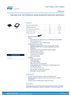
1 Low distortion , Differential ADC Driver data Sheet AD8138 Rev. G Document Feedback Information furnished by analog Devices is believed to be accurate and reliable. However, no responsibility is assumed by analog Devices for its use, nor for any infringements of patents or other rights of third parties that may result from its use. Specifications subject to change without notice. No license is granted by implication or otherwise under any patent or patent rights of analog Devices. Trademarks and registered trademarks are the property of their respective owners. One Technology Way, Box 9106, Norwood, MA 02062-9106, Tel: 1999 2016 analog Devices, Inc. All rights reserved. Technical Support FEATURES Easy to use, single-ended-to- Differential conversion Adjustable output common-mode voltage Externally adjustable gain Low harmonic distortion 94 dBc SFDR at 5 MHz 85 dBc SFDR at 20 MHz 3 dB bandwidth of 320 MHz, G = +1 Fast settling to of 16 ns Slew rate 1150 V/ s Fast overdrive recovery of 4 ns Low input voltage noise of 5 nV/ Hz 1 mV typical offset voltage Wide supply range +3 V to 5 V Low power 90 mW on 5 V dB gain flatness to 40 MHz Available in 8-Lead SOIC and MSOP packages APPLICATIONS ADC drivers Single-ended-to- Differential converters IF and baseband gain blocks Differential buffers Line drivers PIN CONFIGURATION IN1 VOCM2V+3+OUT4+IN8NC7V 6 OUT5NC= NO CONNECTAD813801073-001 Figure 1.
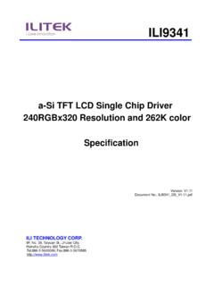
2 TYPICAL APPLICATION CIRCUIT AINAINAVSS499 499 499 499 5V5 VAD8138+ DIGITALOUTPUTSVOCMVINADCVREFAVDDDVDD0107 3-002 Figure 2. GENERAL DESCRIPTION The AD8138 is a major advancement over op amps for Differential signal processing. The AD8138 can be used as a single-ended-to - Differential amplifier or as a Differential -to - Differential amplifier. The AD8138 is as easy to use as an op amp and greatly simplifies Differential signal amplification and driving. Manufactured on the proprietary ADI XFCB bipolar process, the AD8138 has a 3 dB bandwidth of 320 MHz and delivers a Differential signal with the lowest harmonic distortion available in a Differential amplifier. The AD8138 has a unique internal feedback feature that provides balanced output gain and phase matching, suppressing even order harmonics. The internal feedback circuit also minimizes any gain error that would be associated with the mismatches in the external gain setting resistors.
3 The Differential output of the AD8138 helps balance the input to Differential ADCs, maximizing the performance of the ADC. The AD8138 eliminates the need for a transformer with high performance ADCs, preserving the low frequency and dc infor-mation. The common-mode level of the Differential output is adjustable by a voltage on the VOCM pin, easily level-shifting the input signals for driving single-supply ADCs. Fast overload recovery preserves sampling accuracy. The AD8138 distortion performance makes it an ideal ADC Driver for communication systems, with distortion performance good enough to drive state-of-the-art 10-bit to 16-bit converters at high frequencies. The high bandwidth and IP3 of the AD8138 also make it appropriate for use as a gain block in IF and baseband signal chains. The AD8138 offset and dynamic performance makes it well suited for a wide variety of signal processing and data acquisition applications.
4 The AD8138 is available in both SOIC and MSOP packages for operation over 40 C to +85 C temperatures. AD8138 data Sheet Rev. G | Page 2 of 24 TABLE OF CONTENTS Features .. 1 Applications .. 1 Pin Configuration .. 1 Typical Application Circuit .. 1 General Description .. 1 Revision History .. 2 Specifications .. 3 DIN to OUT Specifications .. 3 VOCM to OUT Specifications .. 4 DIN to OUT Specifications .. 5 VOCM to OUT Specifications .. 6 Absolute Maximum Ratings .. 7 Thermal Resistance .. 7 ESD Caution .. 7 Pin Configuration and Function Descriptions .. 8 Typical Performance Characteristics .. 9 Test Circuits .. 15 Operational Description .. 16 Definition of Terms .. 16 Theory of Operation .. 17 Analyzing an Application Circuit .. 17 Setting the Closed-Loop Gain .. 17 Estimating the Output Noise Voltage .. 17 The Impact of Mismatches in the Feedback Networks.
5 18 Calculating the Input Impedance of an Application .. 18 Input Common-Mode Voltage Range in Single-Supply Applications .. 18 Setting the Output Common-Mode Voltage .. 18 Driving a Capacitive Load .. 18 Layout, Grounding, and Bypassing .. 19 Balanced Transformer Driver .. 20 High Performance ADC Driving .. 21 3 V Operation .. 22 Outline Dimensions .. 23 Ordering Guide .. 23 REVISION HISTORY 3/16 Rev. F to Rev. G Changes to Setting the Closed-Loop Gain Section .. 17 Changes to Figure 46 .. 21 Changes to Figure 47 .. 22 1/06 Rev. E to Rev. F Changes to Features .. 1 Added Thermal Resistance Section and Maximum Power Dissipation Section .. 7 Changes to Balanced Transformer Driver Section .. 20 Changes to Ordering Guide .. 23 3/03 Rev. D to Rev. E Changes to Specifications .. 2 Changes to Ordering Guide .. 4 Changes to TPC 16 .. 6 Changes to Table I .. 9 Added New Paragraph after Table I.
6 10 Updated Outline Dimensions .. 14 7/02 Rev. C to Rev. D Addition of TPC 35 and TPC 36 .. 8 6/01 Rev. B to Rev. C Edits to Specifications .. 2 Edits to Ordering Guide .. 4 12/00 Rev. A to Rev. B 9/99 Rev. 0 to Rev. A 3/99 Rev. 0: Initial Version data Sheet AD8138 Rev. G | Page 3 of 24 SPECIFICATIONS DIN TO OUT SPECIFICATIONS At 25 C, VS = 5 V, VOCM = 0, G = +1, RL, dm = 500 , unless otherwise noted. Refer to Figure 39 for test setup and label descriptions. All specifications refer to single-ended input and Differential outputs, unless otherwise noted. Table 1. Parameter Conditions Min Typ Max Unit DYNAMIC PERFORMANCE 3 dB Small Signal Bandwidth VOUT = V p-p, CF = 0 pF 290 320 MHz VOUT = V p-p, CF = 1 pF 225 MHz Bandwidth for dB Flatness VOUT = V p-p, CF = 0 pF 30 MHz Large Signal Bandwidth VOUT = 2 V p-p, CF = 0 pF 265 MHz Slew Rate VOUT = 2 V p-p, CF = 0 pF 1150 V/ s Settling Time , VOUT = 2 V p-p, CF = 1 pF 16 ns Overdrive Recovery Time VIN = 5 V to 0 V step, G = +2 4 ns NOISE/HARMONIC PERFORMANCE1 Second Harmonic VOUT = 2 V p-p, 5 MHz, RL, dm = 800 94 dBc VOUT = 2 V p-p, 20 MHz, RL, dm = 800 87 dBc VOUT = 2 V p-p, 70 MHz, RL, dm = 800 62 dBc Third Harmonic VOUT = 2 V p-p, 5 MHz, RL, dm = 800 114 dBc VOUT = 2 V p-p, 20 MHz, RL, dm = 800 85 dBc VOUT = 2 V p-p, 70 MHz, RL, dm = 800 57 dBc IMD 20 MHz 77 dBc IP3 20 MHz 37 dBm Voltage Noise (RTI)
7 F = 100 kHz to 40 MHz 5 nV/ Hz Input Current Noise f = 100 kHz to 40 MHz 2 pA/ Hz INPUT CHARACTERISTICS Offset Voltage VOS, dm = VOUT, dm/2; VDIN+ = VDIN = VOCM = 0 V 1 + mV TMIN to TMAX variation 4 V/ C Input Bias Current 7 A TMIN to TMAX variation A/ C Input Resistance Differential 6 M Common mode 3 M Input Capacitance 1 pF Input Common-Mode Voltage to + V CMRR VOU T, dm/ VIN, cm; VIN, cm = 1 V 77 70 dB OUTPUT CHARACTERISTICS Output Voltage Swing Maximum VOUT; single-ended output V p-p Output Current 95 mA Output Balance Error VOU T, cm/ VOU T, dm; VOU T, dm = 1 V 66 dB 1 Harmonic distortion performance is equal or slightly worse with higher values of RL, dm. See Figure 17 and Figure 18 for more information. AD8138 data Sheet Rev. G | Page 4 of 24 VOCM TO OUT SPECIFICATIONS At 25 C, VS = 5 V, VOCM = 0, G = +1, RL, dm = 500 , unless otherwise noted.
8 Refer to Figure 39 for test setup and label descriptions. All specifications refer to single-ended input and Differential outputs, unless otherwise noted. Table 2. Parameter Conditions Min Typ Max Unit DYNAMIC PERFORMANCE 3 dB Bandwidth 250 MHz Slew Rate 330 V/ s INPUT VOLTAGE NOISE (RTI) f = MHz to 100 MHz 17 nV/ Hz DC PERFORMANCE Input Voltage Range V Input Resistance 200 k Input Offset Voltage VOS, cm = VOU T, cm; VDIN+ = VDIN = VOCM = 0 V 1 + mV Input Bias Current A VOCM CMRR VOU T, dm/ VOCM; VOCM = 1 V 75 dB Gain VOU T, cm/ VOCM; VOCM = 1 V 1 V/V POWER SUPPLY Operating Range V Quiescent Current 18 20 23 mA TMIN to TMAX variation 40 A/ C Power Supply Rejection Ratio VOU T, dm/ VS; VS = 1 V 90 70 dB OPERATING TEMPERATURE RANGE 40 +85 C data Sheet AD8138 Rev. G | Page 5 of 24 DIN TO OUT SPECIFICATIONS At 25 C, VS = 5 V, VOCM = V, G = +1, RL, dm = 500 , unless otherwise noted.
9 Refer to Figure 39 for test setup and label descriptions. All specifications refer to single-ended input and Differential output, unless otherwise noted. Table 3. Parameter Conditions Min Typ Max Unit DYNAMIC PERFORMANCE 3 dB Small Signal Bandwidth VOUT = V p-p, CF = 0 pF 280 310 MHz VOUT = V p-p, CF = 1 pF 225 MHz Bandwidth for dB Flatness VOUT = V p-p, CF = 0 pF 29 MHz Large Signal Bandwidth VOUT = 2 V p-p, CF = 0 pF 265 MHz Slew Rate VOUT = 2 V p-p, CF = 0 pF 950 V/ s Settling Time , VOUT = 2 V p-p, CF = 1 pF 16 ns Overdrive Recovery Time VIN = V to 0 V step, G = +2 4 ns NOISE/HARMONIC PERFORMANCE1 Second Harmonic VOUT = 2 V p-p, 5 MHz, RL, dm = 800 90 dBc VOUT = 2 V p-p, 20 MHz, RL, dm = 800 79 dBc VOUT = 2 V p-p, 70 MHz, RL, dm = 800 60 dBc Third Harmonic VOUT = 2 V p-p, 5 MHz, RL, dm = 800 100 dBc VOUT = 2 V p-p, 20 MHz, RL, dm = 800 82 dBc VOUT = 2 V p-p, 70 MHz, RL, dm = 800 53 dBc IMD 20 MHz 74 dBc IP3 20 MHz 35 dBm Voltage Noise (RTI)
10 F = 100 kHz to 40 MHz 5 nV/ Hz Input Current Noise f = 100 kHz to 40 MHz 2 pA/ Hz INPUT CHARACTERISTICS Offset Voltage VOS, dm = VOU T, dm/2; VDIN+ = VDIN = VOCM = 0 V 1 + mV TMIN to TMAX variation 4 V/ C Input Bias Current 7 A TMIN to TMAX variation A/ C Input Resistance Differential 6 M Common mode 3 M Input Capacitance 1 pF Input Common-Mode Voltage to + V CMRR VOUT, dm/ VIN, cm; VIN, cm = 1 V 77 70 dB OUTPUT CHARACTERISTICS Output Voltage Swing Maximum VOUT; single-ended output V p-p Output Current 95 mA Output Balance Error VOU T, cm/ VOU T, dm; VOU T, dm = 1 V 65 dB 1 Harmonic distortion performance is equal or slightly worse with higher values of RL, dm. See Figure 17 and Figure 18 for more information. AD8138 data Sheet Rev. G | Page 6 of 24 VOCM TO OUT SPECIFICATIONS At 25 C, VS = 5 V, VOCM = V, G = +1, RL, dm = 500 , unless otherwise noted.