Transcription of LOW DROPOUT LINEAR REGULATOR - Diodes Incorporated
1 AZ1117C Document number: DS36676 Rev. 4 - 2 1 of 23 January 2019 Diodes Incorporated AZ1117C LOW DROPOUT LINEAR REGULATOR Description The AZ1117C is a low DROPOUT three-terminal REGULATOR . The AZ1117C has been optimized for low voltage where transient response and minimum input voltage are critical. It provides current limit and thermal shutdown. Its circuit includes a trimmed bandgap reference to assure output voltage accuracy to be within 1%. On-chip thermal shutdown provides protection against a combination of high current and ambient temperature that would create excessive junction temperature. The AZ1117C is available in , , , , , fixed output voltage versions and ADJ output voltage version. The fixed versions integrate the adjust resistors. It is also available in an adjustable version which can set the output voltage with two external resistors.
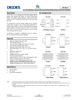
2 The AZ1117C is available in the industry-standard TO252-2 Series (including TO252-2 (3), TO252-2 (4), and TO252-2 (5)), SOT89 and SOT223 power packages. Features Current Limit: (Typ) Output Noise from 10Hz to 10kHz: of VOUT PSRR at IOUT = 300mA and f = 120Hz: 70dB Output Voltage Accuracy: 1% (Except Version) On-chip Thermal Shutdown Maximum Quiescent Current: IQMAX = 6mA Compatible with Low ESR Ceramic Capacitor Operation Junction Temperature: -20 C to +125 C Totally Lead-Free & Fully RoHS Compliant (Notes 1 & 2) Halogen and Antimony Free. Green Device (Note 3) Applications USB Device Add-on Card DVD Player PC Motherboard Notes: 1. No purposely added lead. Fully EU Directive 2002/95/EC (RoHS), 2011/65/EU (RoHS 2) & 2015/863/EU (RoHS 3) compliant. 2. See for more information about Diodes Incorporated s definitions of Halogen- and Antimony-free, "Green" and Lead-free.
3 3. Halogen- and Antimony-free "Green products are defined as those which contain <900ppm bromine, <900ppm chlorine (<1500ppm total Br + Cl) and <1000ppm antimony compounds. Pin Assignments (Top View) (Top View) TO252-2 (3) Option 1 TO252-2 (3) Option 2 (Top View) (Top View) TO252-2 (4) TO252-2 (5) 123 INPUTOUTPUTADJ/GNDINPUTOUTPUTADJ/GNDVOUT 123123 INPUTOUTPUTADJ/GND123 INPUTOUTPUTADJ/GND AZ1117C Document number: DS36676 Rev.
4 4 - 2 2 of 23 January 2019 Diodes Incorporated AZ1117C Pin Assignments (Cont.) (Top View) (Top View) SOT89 Option 1/ R Package SOT89 Option 2/ R Package (Top View) (Top View) SOT89 Option 1/ R2 Package SOT89 Option 2/ R2 Package (Top View)
5 (Top View) SOT223/ H Package SOT223/ H2 Package VOUTINPUTOUTPUTADJ/GND123 INPUTOUTPUTADJ/GND123 ADJ/GND123 VININPUTOUTPUTADJ/GNDVININPUTOUTPUTADJ/G ND123123 VOUTINPUTOUTPUTADJ/GNDVOUTINPUTOUTPUTADJ /GND123 AZ1117C Document number: DS36676 Rev. 4 - 2 3 of 23 January 2019 Diodes Incorporated AZ1117C Typical Applications Circuit (Note 4) AZ1117C-ADJINPUTOUTPUTADJVIN=11V R1124 R29V * (1+R2/R1)+IADJ*R2 10 F VIN= F768 22 F22 Note 4: The AZ1117C is compatible with low ESR ceramic capacitor. The ESR of the output capacitors must be less than 20 . A minimum of 10 F output capacitor is required. Functional Block Diagram A(B){C} A for TO252-2 Series/SOT223 (H)/SOT89 (R) B for SOT89 (R2) C for SOT223 (H2) ThermalProtection+-For Adjustable Output, disconnect A1 and A2, connect BINPUTOUTPUTADJ/GNDA1A2 BFor Fixed Output, connect A1 and A2, disconnect B3(2){1} 2(3){3} 1(1){2} AZ1117C Document number: DS36676 Rev.
6 4 - 2 4 of 23 January 2019 Diodes Incorporated AZ1117C Absolute Maximum Ratings (Note 5) Symbol Parameter Rating Unit VIN Input Voltage 18 V TJ Operating Junction Temperature Range +150 C TSTG Storage Temperature Range -65 to +150 C JA Thermal Resistance (Without Heatsink) SOT89 170 C/W SOT223 125 TO252-2 Series 100 JA Thermal Resistance (With Heatsink) (Note 6) SOT89 150 C/W SOT223 100 TO252-2 Series 70 TLEAD Lead Temperature (Soldering, 10sec) +260 C ESD (Human Body Model) 4000 V Notes: 5. Stresses greater than those listed under Absolute Maximum Ratings may cause permanent damage to the device. These are stress ratings only, and functional operation of the device at these or any other conditions beyond those indicated under Recommended Operating Conditions is not implied.
7 Exposure to Absolute Maximum Ratings for extended periods may affect device reliability. 6. Chip is soldered to 100mm2(10mm*10mm) copper (top side solder mask) on layers FR-4 PCB with 8* vias. Recommended Operating Conditions Symbol Parameter Min Max Unit VIN Input Voltage 15 V TJ Operating Junction Temperature Range -20 +125 C Electrical Characteristics AZ1117C-ADJ (Operating Conditions: VIN = VOUT+2V, IOUT = 10mA, TJ = +25 C, unless otherwise specified. (P maximum power dissipation). Limits appearing in Boldface type apply over the entire junction temperature range for operation, -20 C to +125 C.) Symbol Parameter Conditions Min Typ Max Unit VREF Reference Voltage VIN-VOUT 10V V VRLINE Line Regulation VIN-VOUT 10V % VRLOAD Load Regulation % VDROP DROPOUT Voltage VREF = 1%, IOUT = SOT223 V TO252-2 Series V ILIMIT Current Limit 1 A Adjust Pin Current 60 120 A Adjust Pin Current Change (VIN-VOUT) 10V 5 A Minimum Load Current (VIN-VOUT) 10V 5 mA PSRR Ripple Rejection f = 120Hz, COUT = 22 F (VIN-VOUT) = 3V, IOUT = 300mA 70 dB Temperature Stability % RMS Output Noise (% of VOUT) TA = +25 C, 10Hz f 10kHz % Thermal Shutdown Junction Temperature +160 C Thermal Shutdown Hysteresis +16 C JC Thermal Resistance (Junction to Case)
8 SOT89 30 C/W SOT223 15 TO252-2 Series 10 AZ1117C Document number: DS36676 Rev. 4 - 2 5 of 23 January 2019 Diodes Incorporated AZ1117C Electrical Characteristics (Cont.) (Operating Conditions: VIN 10V, IOUT = 10mA, TJ = +25 C, unless otherwise specified. (P maximum power dissipation). Limits appearing in Boldface type apply over the entire junction temperature range for operation, -20 C to +125 C.) Symbol Parameter Conditions Min Typ Max Unit VOUT Output Voltage VIN-VOUT 10V V VRLINE Line Regulation VIN-VOUT 10V 6 mV 10 VRLOAD Load Regulation 2 15 mV VDROP DROPOUT Voltage VOUT = 1%, IOUT = SOT223 V TO252-2 Series V ILIMIT Current Limit 1 A IQ Quiescent Current IOUT = 0 4 6 mA PSRR Ripple Rejection f = 120Hz, COUT = 22 F (VIN-VOUT) = 3V, IOUT = 300mA 70 dB Temperature Stability % RMS Output Noise (% of VOUT) TA = +25 C, 10Hz f 10kHz % Thermal Shutdown Junction Temperature +160 C Thermal Shutdown Hysteresis +16 C JC Thermal Resistance (Junction to Case) SOT89 30 C/W SOT223 15 TO252-2 Series 10 Electrical Characteristics (Cont.)
9 (Operating Conditions: VIN 10V, IOUT = 10mA, TJ = +25 C, unless otherwise specified. (P maximum power dissipation). Limits appearing in Boldface type apply over the entire junction temperature range for operation, -20 C to +125 C.) Symbol Parameter Conditions Min Typ Max Unit VOUT Output Voltage VIN-VOUT 10V V VRLINE Line Regulation VIN-VOUT 10V 6 mV 10 VRLOAD Load Regulation 2 15 mV VDROP DROPOUT Voltage VOUT = 1%, IOUT = SOT223 V TO252-2 Series V ILIMIT Current Limit 1 A IQ Quiescent Current IOUT = 0 4 6 mA PSRR Ripple Rejection f = 120Hz, COUT = 22 F (VIN-VOUT) = 3V, IOUT = 300mA 70 dB Temperature Stability % RMS Output Noise (% of VOUT) TA = +25 C, 10Hz f 10kHz % Thermal Shutdown Junction Temperature +160 C Thermal Shutdown Hysteresis +16 C JC Thermal Resistance (Junction to Case) SOT89 30 C/W SOT223 15 TO252-2 Series 10 AZ1117C Document number: DS36676 Rev.
10 4 - 2 6 of 23 January 2019 Diodes Incorporated AZ1117C Electrical Characteristics (Cont.) (Operating Conditions: VIN 10V, IOUT = 10mA, TJ = +25 C, unless otherwise specified. (P maximum power dissipation). Limits appearing in Boldface type apply over the entire junction temperature range for operation, -20 C to +125 C.) Symbol Parameter Conditions Min Typ Max Unit VOUT Output Voltage VIN-VOUT 10V V VRLINE Line Regulation VIN-VOUT 10V 6 mV 10 VRLOAD Load Regulation 2 15 mV VDROP DROPOUT Voltage VOUT = 1%, IOUT = SOT223 V TO252-2 Series V ILIMIT Current Limit 1 A IQ Quiescent Current IOUT = 0 4 6 mA PSRR Ripple Rejection f = 120Hz, COUT = 22 F (VIN-VOUT) = 3V, IOUT = 300mA 70 dB Temperature Stability % RMS Output Noise (% of VOUT) TA = +25 C, 10Hz f 10kHz % Thermal Shutdown Junction Temperature +160 C Thermal Shutdown Hysteresis +16 C JC Thermal Resistance (Junction to Case) SOT89 30 C/W SOT223 15 TO252-2 Series 10 Electrical Characteristics (Cont.)