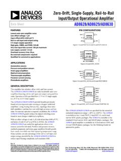
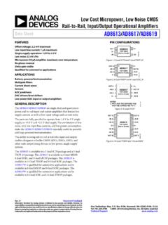
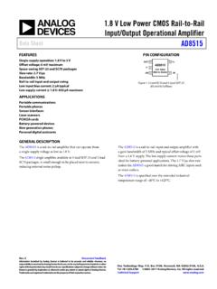
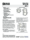
Transcription of Low Power, Low Noise and Distortion, Rail-to-Rail Output ...
1 Low Power, Low Noise and Distortion, Rail-to-Rail Output Amplifiers Data Sheet ada4841 -1/ ada4841 -2 Rev. G Document Feedback Information furnished by Analog Devices is believed to be accurate and reliable. However, no responsibility is assumed by Analog Devices for its use, nor for any infringements of patents or other rights of third parties that may result from its use. Specifications subject to change without notice. No license is granted by implication or otherwise under any patent or patent rights of Analog Devices. Trademarks and registered trademarks are the property of their respective owners. One Technology Way, Box 9106, Norwood, MA 02062-9106, Tel: 2005 2017 Analog Devices, Inc.
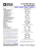
2 All rights reserved. Technical Support FEATURES Low power: mA/amp Low wideband Noise nV/ Hz pA/ Hz Low 1/f Noise 7 nV/ Hz @ 10 Hz 13 pA/ Hz @ 10 Hz Low distortion: 105 dBc @ 100 kHz, VO = 2 V p-p High speed 80 MHz, 3 dB bandwidth (G = +1) 12 V/ s slew rate 175 ns settling time to Low offset voltage: mV maximum Rail-to-Rail Output Power down Wide supply range: V to 12 V APPLICATIONS Low power, low Noise signal processing Battery-powered instrumentation 16-bit PulSAR ADC drivers CONNECTION DIAGRAMS VOUT34652718 VS IN+IN+VSNCNCPOWER DOWN05614-001 ada4841 -1 TOP VIEW(Not to Scale) Figure 1. 8-Lead SOIC (R) VOUT1 VS2+IN3+VS6 POWER DOWN5 IN4 ada4841 -105614-099 Figure 2.
3 6-Lead SOT-23 (RJ) OUT11 IN12+IN13 VS4+VS8 OUT27 IN26+IN25 ada4841 -2 TOP VIEW(Not to Scale)05614-064 NOTES1. FOR 8-LEAD LFCSP_WD, CONNECT EXPOSED PADDLE TO GND. Figure 3. 8-Lead MSOP (RM), 8-Lead SOIC_N (R), and 8-Lead LFCSP_WD (CP) GENERAL DESCRIPTION The ada4841 -1/ ada4841 -2 are unity gain stable, low Noise and distortion, Rail-to-Rail Output amplifiers that have a quiescent current of mA maximum. In spite of their low power consumption, these amplifiers offer low wideband voltage Noise performance of nV/ Hz and pA/ Hz current Noise , along with excellent spurious-free dynamic range (SFDR) of 105 dBc at 100 kHz. To maintain a low Noise environment at lower frequencies, the amplifiers have low 1/f Noise of 7 nV/ Hz and 13 pA/ Hz at 10 Hz.
4 The ada4841 -1/ ada4841 -2 Output can swing to less than 50 mV of either rail. The input common-mode voltage range extends down to the negative supply. The ada4841 -1/ ada4841 -2 can drive up to 10 pF of capacitive load with minimal peaking. The ada4841 -1/ ada4841 -2 provide the performance required to efficiently support emerging 16-bit to 18-bit ADCs and are ideal for portable instrumentation, high channel count, industrial measurement, and medical applications. The ada4841 -1/ ada4841 -2 are ideally suited to drive the AD7685/AD7686, 16-bit PulSAR ADCs. The ada4841 -1/ ada4841 -2 packages feature RoHS compliant lead finishes. The amplifiers are rated to work over the industrial temperature range ( 40 C to +125 C).
5 30 (MHz)HARMONIC DISTORTION (dBc) p-p THIRD 40 50 60 70 80 90 100 110VS = 5VG = +12V p-p SECOND Figure 4. Harmonic Distortion ada4841 -1/ ada4841 -2 Data Sheet Rev. G | Page 2 of 20 TABLE OF CONTENTS Features .. 1 Applications .. 1 Connection Diagrams .. 1 General Description .. 1 Revision History .. 2 Specifications .. 3 Absolute Maximum Ratings .. 6 Thermal Resistance .. 6 Maximum Power Dissipation .. 6 ESD Caution .. 6 Typical Performance Characteristics .. 7 Theory of Operation .. 13 Amplifier Description .. 13 DC Errors .. 13 Noise Considerations .. 13 Headroom Considerations .. 14 Capacitance Drive .. 15 Input Protection .. 15 Power-Down Operation .. 16 Applications Information.
6 17 Typical Performance Values .. 17 16-Bit ADC Driver .. 17 Reconstruction Filter .. 17 Layout Considerations .. 18 Ground Plane .. 18 Power Supply Bypassing .. 18 Outline Dimensions .. 19 Ordering Guide .. 20 REVISION HISTORY 3/2017 Rev. F to Rev. G Updated Outline Dimensions .. 20 Changes to Ordering Guide .. 20 3/2014 Rev. E to Rev. F Changes to Figure 14 .. 8 Updated Outline Dimensions .. 20 Changes to Ordering Guide .. 20 12/2010 Rev. D to Rev. E Changes to negative Power Supply Rejection Ration Conditions .. 3 Changes to Ordering Guide .. 20 1/2010 Rev. C to Rev. D Added LFCSP Package .. Universal Changes to Operating Temperature Range Parameter, Ta b l e 4 .. 6 Updated Outline Dimensions.
7 19 Changes to Ordering Guide .. 20 3/2006 Rev. B to Rev. C Added SOT-23 Package .. Universal Changes to General Description .. 1 Changes to Table 1 .. 3 Changes to Table 2 .. 4 Changes to Table 3 .. 5 Changes to Input Protection Section .. 15 Changes to Ordering Guide .. 20 10/2005 Rev. A to Rev. B Added ada4841 -2 .. Universal Changes to General Description and Features .. 1 Changes to Table 1 .. 3 Changes to Table 2 .. 4 Changes to Table 3 .. 5 Changes to Table 4, Table 5, and Figure 4 .. 6 Changes to Figure 6 .. 7 Changes to Figure 12, Figure 13, Figure 15, and Figure 16 .. 8 Deleted Figure 25; Renumber 10 Changes to Figure 24 and Figure 28 .. 10 Changes to Figure 31 .. 11 Inserted Figure 37; Renumber Sequentially.
8 12 Changes to Amplifier Description Section and Figure 39 .. 13 Changed DC Performance Considerations Section to DC Errors Section .. 13 Changes to Noise Considerations Section .. 14 Changes to Headroom Considerations Section and Figure 39 15 Changes to Power-Down Operation Section .. 16 Changes to 16-Bit ADC Driver Section, Figure 48, and Figure 49 17 Changes to Power Supply Bypassing Section .. 18 Updated Outline Dimensions .. 19 Changes to Ordering Guide .. 20 9/2005 Rev. 0 to Rev. A Changes to Features .. 1 Changes to Figure 2 .. 1 Changes to Figure 12 .. 8 Changes to Figure 40 .. 14 Changes to Headroom Considerations Section .. 15 7/2005 Revision 0: Initial Version Data Sheet ada4841 -1/ ada4841 -2 Rev.
9 G | Page 3 of 20 SPECIFICATIONS TA = 25 C, VS = 5 V, RL = 1 k , Gain = +1, unless otherwise noted. Table 1. Parameter Conditions Min Typ Max Unit DYNAMIC PERFORMANCE 3 dB Bandwidth VO = V p-p 58 80 MHz VO = 2 V p-p 3 MHz Slew Rate G = +1, VO = 9 V step, RL = 1 k 12 13 V/ s Settling Time to G = +1, VO = 8 V step 650 ns Settling Time to G = +1, VO = 8 V step 1000 ns Noise /HARMONIC PERFORMANCE Harmonic Distortion HD2/HD3 fC = 100 kHz, VO = 2 V p-p, G = +1 111/ 105 dBc fC = 1 MHz, VO = 2 V p-p 80/ 67 dBc Input Voltage Noise f = 100 kHz nV/ Hz Input Current Noise f = 100 kHz pA/ Hz DC PERFORMANCE Input Offset Voltage 40 300 V Input Offset Voltage Drift 1 V/ C Input Bias Current 3 A Input Offset Current A Open-Loop Gain VO = 4 V 103 120 dB INPUT CHARACTERISTICS Input Resistance, Common Mode 90 M Input Resistance, Differential Mode 25 k Input Capacitance, Common Mode 1 pF Input Capacitance, Differential Mode 3 pF Input Common-Mode Voltage Range +4 V Common-Mode Rejection Ratio (CMRR) VCM = 4 V 95 115 dB MATCHING CHARACTERISTICS ( ada4841 -2)
10 Input Offset Voltage 70 V Input Bias Current 60 nA POWER DOWN PIN ( ada4841 -1) POWER DOWN Voltage Enabled > V POWER DOWN Voltage Power down < V Input Current Enable POWER DOWN = +5 V 1 2 A Power Down POWER DOWN = 5 V 13 30 A Switching Speed Enable 1 s Power Down 40 s Output CHARACTERISTICS Output Voltage Swing G > +1 V Output Current Limit Sourcing, VIN = +VS , RL = 50 to GND 30 mA Sinking, VIN = VS , RL = 50 to GND 60 mA Capacitive Load Drive 30% overshoot 15 pF POWER SUPPLY Operating Range 12 V Quiescent Current/Amplifier POWER DOWN = +5 V mA POWER DOWN = 5 V 40 90 A Positive Power Supply Rejection Ratio +VS = +5 V to +6 V.
