Transcription of LT1021 - Precision Reference
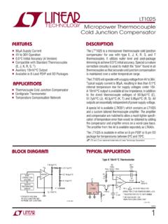
1 1LT10211021fcAPPLICATIO SUFEATURESTYPICAL APPLICATIOUDESCRIPTIOUP recision ReferenceTypical Distribution of Temperature DriftOUTPUT DRIFT (ppm/ C) 5 UNITS (%)2421181512963 031021 TA01 3 1152 4 204 DISTRIBUTION OF THREE RUNSB asic Positive and Negative ConnectionsLT1021 OUTIN GNDLT1021(7 AND 10 ONLY)OUTIN GNDVOUT VOUTVINNCR1 = VOUT (V )ILOAD + 15V(V )R11021 TA01 Ultralow Drift: 5ppm/ C Max Slope Very Low Noise: <1ppm P-P ( to 10Hz) 100% Noise Tested Pin Compatible with Most bandgap ReferenceApplications, Including Ref 01, Ref 02, LM368,MC1400 and MC1404 with Greatly ImprovedStability, Noise and Drift Trimmed Output voltage Operates in Series or Shunt Mode Output Sinks and Sources in Series Mode >100dB Ripple Rejection Minimum Input/Output Differential of 1V Available in 5-Lead Can, N8 and S8 Packages A/D and D/A Converters Precision Regulators Digital Voltmeters Inertial Navigation Systems Precision Scales Portable Reference StandardThe LT 1021 is a Precision Reference with ultralow driftand noise, extremely good long term stability and almosttotal immunity to input voltage variations.
2 The referenceoutput will both source and sink up to 10mA. Threevoltages are available: 5V, 7V and 10V. The 7V and 10 Vunits can be used as shunt regulators (two-terminal zeners)with the same Precision characteristics as the three-terminal connection. Special care has been taken to mini-mize thermal regulation effects and temperatureinduced LT1021 references are based on a buried zener diodestructure that eliminates noise and stability problemsassociated with surface breakdown devices. Further, asubsurface zener exhibits better temperature drift andtime stability than even the best bandgap circuit design makes the LT1021 the first ICreference to offer ultralow drift without the use of highpower on-chip LT1021 -7 uses no resistive divider to set outputvoltage, and therefore exhibits the best long term stabilityand temperature hysteresis.
3 The LT1021 -5 and LT1021 -10 are intended for systems requiring a precise 5V or 10 Vreference with an initial tolerance as low as , LTC and LT are registered trademarks of Linear Technology other trademarks are the property of their respective voltage .. 40 VInput/Output voltage Differential .. 35 VOutput-to-Ground voltage (Shunt Mode Current Limit) LT1021 -5 .. 10 VLT1021-7 .. 10 VLT1021-10 .. 16 VTrim Pin-to-Ground VoltagePositive .. Equal to VOUTN egative .. 20 VOutput Short-Circuit DurationVIN = 35V .. 10 secVIN 20V .. IndefiniteOperating Temperature RangeCommercial .. 0 C to 70 CIndustrial .. 40 C to 85 CMilitary .. 55 C to 125 CStorage Temperature Range.
4 65 C to 150 CLead Temperature (Soldering, 10 sec) .. 300 CWUUPACKAGE/ORDER I FOR ATIOTJMAX = 150 C, JA = 150 C/ W, JC = 45 C/WTOP VIEWNC*NC*NC*VINVOUTTRIM**NC*GND87653214 H PACKAGE8-LEAD TO-5 METAL CANTJMAX = 130 C, JA = 130 C/W (N)TJMAX = 130 C, JA = 150 C/ W (S)(Note 1)12348765 TOP VIEWDNC*VINDNC*GNDDNC*DNC*V0 UTTRIM**N8 PACKAGE8-LEAD PDIPS8 PACKAGE8-LEAD PLASTIC SO *CONNECTED INTERNALLY. DO NOT CONNECT EXTERNAL CIRCUITRY TO THESE PINS.**NO TRIM PIN ON LT1021 -7. DO NOT CONNECT EXTERNAL CIRCUITRY TO PIN 5 ON LT1021 -7 ORDER PART NUMBER *CONNECTED INTERNALLY. DO NOT CONNECT EXTERNAL CIRCUITRY TO THESE PINS.**NO TRIM PIN ON LT1021 -7. DO NOT CONNECT EXTERNAL CIRCUITRY TO PIN 5 ON LT1021 -7 OBSOLETELT1021 BCH-5LT1021 BMH-5LT1021 CCH-5LT1021 CMH-5LT1021 BMH-10LT1021 DCH-5LT1021 DMH-5LT1021 BCH-7LT1021 BMH-7LT1021 DCH-7LT1021 DMH-7LT1021 BCH-10LT1021 CMH-10LT1021 DCH-10LT1021 DMH-10LT1021 BCN8-5LT1021 CCN8-5LT1021 CIN8-5LT1021 DCN8-5LT1021 DIN8-5LT1021 BCN8-7LT1021 DCN8-7LT1021 BCN8-10LT1021 CCN8-10LT1021 CIN8-10LT1021 DCN8-10LT1021 DIN8-10210521072110N8 ORDER PART NUMBERLT1021 DCS8-5LT1021 DCS8-7LT1021 DCS8-10S8 ORDER PART NUMBERS8 PART MARKINGO rder Options Tape and Reel: Add #TRLead Free: Add #PBF Lead Free Tape and Reel: Add #TRPBFLead Free Part Marking.
5 LTC Marketing for parts specified with wider operating temperature CCHARA TERISTICSLT1021-5 PARAMETERCONDITIONSMINTYPMAXUNITSO utput voltage (Note 2) voltage Temperature Coefficient (Note 3)TMIN TJ TMAXLT1021B-5 25ppm/ CLT1021C-5/LT1021D-5 320ppm/ CLine Regulation (Note 4) VIN 10V412ppm/V 20ppm/V10V VIN 40V26ppm/V 10ppm/VLoad Regulation (Sourcing Current)0 IOUT 10mA1020ppm/mA(Note 4) 35ppm/mALoad Regulation (Sinking Current)0 IOUT 10mA60100ppm/mA(Note 4) 150ppm/mASupply voltage Noise (Note 6) f VP-P10Hz f VRMSLong Term Stability of Output voltage (Note 7) t = 1000 Hrs Noncumulative15ppmTemperature Hysteresis of Output T = 25 C10ppmLT1021-7 PARAMETERCONDITIONSMINTYPMAXUNITSO utput voltage (Note 2) voltage Temperature Coefficient (Note 3)TMIN TJ TMAXLT1021B-7 25ppm/ CLT1021D-7 320ppm/ CLine Regulation (Note 4) VIN VIN Regulation (Sourcing Current)0 IOUT 10mA1225ppm/mA(Note 4) 40ppm/mALoad Regulation (Shunt Mode) ISHUNT 10mA50100ppm/mA(Notes 4, 5) 150ppm/mASupply Current (Series Mode) Current (Shunt Mode)VIN is voltage Noise (Note 6) f VP-P10Hz f VRMSLong Term Stability of Output voltage (Note 7)
6 T = 1000 Hrs Noncumulative7ppmTemperature Hysteresis of Output T = 25 C3ppmThe denotes specifications that apply over the full operating temperaturerange, otherwise specifications are TA = 25 C. VIN = 10V, IOUT = 0, unless otherwise denotes specifications that apply over the full operating temperature range, otherwise specifications are TA = 25 = 12V, IOUT = 0, unless otherwise CCHARA TERISTICSLT1021-10 PARAMETERCONDITIONSMINTYPMAXUNITSO utput voltage (Note 2) voltage Temperature Coefficient (Note 3)TMIN TJ TMAXLT1021B-10 25ppm/ CLT1021C-10/LT1021D-10 520ppm/ CLine Regulation (Note 4) VIN 6 VIN 4ppm/VLoad Regulation (Sourcing Current)0 IOUT 10mA1225ppm/mA(Note 4) 40ppm/mALoad Regulation (Shunt Mode) ISHUNT 10mA50100ppm/mA(Notes 4, 5) 150ppm/mASupply Current (Series Mode) Current (Shunt Mode)VIN is voltage Noise (Note 6)
7 F VP-P10Hz f VRMSLong Term Stability of Output voltage (Note 7) t = 1000 Hrs Noncumulative15ppmTemperature Hysteresis of Output T = 25 C5ppmNote 1: Absolute Maximum Ratings are those values beyond which the lifeof a device may be 2: Output voltage is measured immediately after turn-on. Changesdue to chip warm-up are typically less than 3: Temperature coefficient is measured by dividing the change inoutput voltage over the temperature range by the change in tests are done for hot and cold; TMIN to 25 C and 25 C to slope is also measured at 25 4: Line and load regulation are measured on a pulse basis. Outputchanges due to die temperature change must be taken into accountseparately.
8 Package thermal resistance is 150 C/W for TO-5 (H), 130 C/Wfor N and 150 C/W for the 5: Shunt mode regulation is measured with the input open. With theinput connected, shunt mode current can be reduced to 0mA. Loadregulation will remain the 6: RMS noise is measured with a 2-pole highpass filter at 10Hz and a2-pole lowpass filter at 1kHz. The resulting output is full-wave rectified andthen integrated for a fixed period, making the final reading an average asopposed to RMS. Correction factors are used to convert from average toRMS and correct for the non-ideal bandpass of the noise is measured with a single highpass filter at and a2-pole lowpass filter at 10Hz. The unit is enclosed in a still-air environmentto eliminate thermocouple effects on the leads.
9 Test time is 10 7: Consult factory for units with long term stability denotes specifications that apply over the full operating temperaturerange, otherwise specifications are TA = 25 C. VIN = 15V, IOUT = 0, unless otherwise TERISTICSUWATYPICALPERFORCES tart-Up (Series Mode)Ripple RejectionINPUT voltage (V)085 REJECTION (dB)909510010510203040LT1021 G011101155152535f = 150 HzLT1021-5LT1021-10LT1021-7 TIME ( s)3 OUTPUT voltage (V)46781310268LT1021 G0451112904101214LT1021-10LT1021-5LT1021 -7 VIN = 0V TO 12 VOutput voltage Noise SpectrumOUTPUT CURRENT (mA)0 INPUT/OUTPUT voltage (V) = 125 CTJ = 55 CTJ = 25 CFREQUENCY (Hz)100 NOISE voltage (nV/ Hz)200250350400101k10kLT1021 G06010030015050LT1021-10LT1021-5LT1021-7 Ripple RejectionFREQUENCY (Hz)1090 REJECTION (dB)
10 11013012010080601001k10kLT1021 G027050 VIN = 15 VCOUT = 0LT1021-5LT1021-10LT1021-7 Start-Up (Shunt Mode) LT1021 -7, LT1021 -10 TIME ( s)OUTPUT voltage (V)9101148LT1021 G0587026101265LT1021-10LT1021-7IN GNDOUTNC1kVOUT0 VVOUT + 2 VBANDWIDTH (Hz)108 RMS NOISE ( V)12161410621001k10kLT1021 G0740 COUT = 0 FILTER = 1 POLEfLOW = voltage Temperature DriftLT1021-5 Output voltage NoiseTEMPERATURE ( C) voltage (V) 2525100125 Load Regulation LT1021 -5 OUTPUT CURRENT (mA) 10 OUTPUT CHANGE (mV)135420 2 46LT1021 G09 1 3 5 6 8 4048 2210 VIN = 8 VSOURCINGSINKINGM inimum Input/Output DifferentialLT1021-7, LT1021 -106LT10211021fcCCHARA TERISTICSUWATYPICALPERFORCEQ uiescent Current LT1021 -5 INPUT voltage (V)00 INPUT CURRENT (mA) = 55 CTJ = 25 CTJ = 125 CIOUT = 0 Sink Mode* Current LimitLT1021-5 OUTPUT voltage (V)00 CURRENT INTO OUTPUT (mA)10304050481018LT1021 G11202612141660 VIN = 8V*NOTE THAT AN INPUT voltage IS REQUIRED FOR 5V Regulation LT1021 -5 TIME (ms)OUTPUT CHANGE (mV) G122060100004080120 LOADREGULATIONTHERMAL REGULATIONILOAD = 10mAVIN = 25V POWER = 200mWLoad Transient ResponseLT1021-5, CLOAD = 1000pFLoad Transient ResponseLT1021-5, CLOAD = 0 TIME ( s)
