Transcription of LT1028/LT1128 - Ultralow Noise Precision High Speed Op Amps
1 LT1028/LT112811028fdFor more information APPLICATION FEATURESDESCRIPTIONU ltralow Noise PrecisionHigh Speed Op AmpsThe LT 1028(gain of 1 stable)/LT1128(gain of +1 stable) achieve a new standard of excellence in Noise performance with Hz 1kHz Noise , Hz 10Hz Noise . This Ultralow Noise is combined with excellent high Speed specifications (gain-bandwidth product is 75 MHz for LT1028, 20 MHz for LT1128), distortion-free output, and true Precision parameters ( V/ C drift, 10 V offset voltage, 30 million voltage gain). Although the LT1028/LT1128 input stage operates at nearly 1mA of collector current to achieve low voltage Noise , input bias current is only LT1028/LT1128 s voltage Noise is less than the Noise of a 50 resistor. Therefore, even in very low source impedance transducer or audio amplifier applications, the LT1028/LT1128 s contribution to total system Noise will be , LT, LT C, LT M, Linear Technology and the Linear logo are registered trademarks of Linear Technology Corporation.
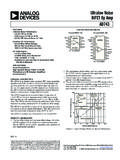
2 All other trademarks are the property of their respective Noise 1M TIA Photodiode AmplifierAPPLICATIONSn Voltage Noise Hz Max at 1kHz Hz Typ at 1kHz Hz Typ at 10Hz 35nVP-P Typ, to 10 Hzn Voltage and Current Noise 100% Testedn Gain-Bandwidth Product LT1028: 50 MHz Min LT1128: 13 MHz Minn Slew Rate LT1028: 11V/ s Min LT1128: 5V/ s Minn Offset Voltage: 40 V Maxn Drift with Temperature: V/ C Maxn Voltage Gain: 7 Million Minn Available in 8-Lead SO Packagen Low Noise Frequency Synthesizersn High Quality Audion Infrared Detectorsn Accelerometer and gyro Amplifiersn 350 Bridge signal Conditioningn Magnetic Search Coil Amplifiersn Hydrophone AmplifiersVoltage Noise vs FrequencyFREQUENCY (Hz) TA02 VOLTAGE Noise DENSITY (nV/ Hz) CORNER = CORNER = 14 HzTYPICALMAXIMUMVS = 15 VTA = 25 C+ VOUT = ~ + IPD 1 MVS VS VS+ = 15 VLT1028/LT112821028fdFor more information MAXIMUM RATINGSS upply Voltage 55 C to 105 C.
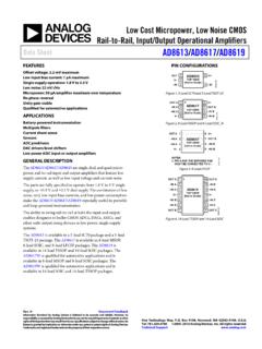
3 22V 105 C to 125 C .. 16 VDifferential Input Current (Note 9) .. 25mAInput Voltage ..Equal to Supply VoltageOutput Short-Circuit Duration ..Indefinite(Note 1)TOP VIEWV+VOS TRIM INOUTOVER-COMP+INV (CASE)8753214H PACKAGE8-LEAD TO-5 METAL CANVOS TRIM+ 6 TJMAX = 175 C, JA = 140 C/W, JC = 40 C/W OBSOLETE PACKAGE12345678 TOP VIEW IN+INV S8 PACKAGE8-LEAD PLASTIC SOICV+OUT+ VOSTRIMVOSTRIMOVER-COMP TJMAX = 150 C, JA = 140 C/WN8 PACKAGE8-LEAD PLASTIC DIP12345678 TOP VIEW IN+INV V+OUT+ OVER-COMPVOSTRIMVOSTRIM TJMAX = 150 C, JA = 150 C/WTOP VIEWSW PACKAGE16-LEAD PLASTIC SOL12345678161514131211109 NCNCTRIM IN+INV NCNCNCNCTRIMV+OUTNCNCOVER-COMP+ TJMAX = 150 C, JA = 130 C/WNOTE: THIS DEVICE IS NOT RECOMMENDED FOR NEW DESIGNSJ8 PACKAGE8-LEAD CERAMIC DIPTJMAX = 175 C, JA = 140 C/W, JC = 40 C/W OBSOLETE PACKAGEPIN CONFIGURATIONO perating Temper atur e Range LT1028/LT1128AM, M (OBSOLETE) .. 55 C to 125 C LT1028/LT1128AC, C (Note 11).
4 40 C to 85 CStorage Temper atur e Range All Devices .. 65 C to 150 CLead Temper atur e (Soldering, 10 sec.) ..300 CLT1028/LT112831028fdFor more information INFORMATIONLEAD FREE FINISHTAPE AND REELPART MARKING*PACKAGE DESCRIPTIONSPECIFIED TEMPERATURE RANGELT1028 ACN8#PBFN/ALT1028 ACN88-Lead PDIP0 C to 70 CLT1028CN8#PBFN/ALT1028CN88-Lead PDIP0 C to 70 CLT1128 ACN8#PBFN/ALT1128 ACN88-Lead PDIP0 C to 70 CLT1128CN8#PBFN/ALT1128CN88-Lead PDIP0 C to 70 CLT1028CS8#PBFLT1028CS8#TRPBF10288-Lead Plastic Small Outline0 C to 70 CLT1128CS8#PBFLT1128CS8#TRPBF11288-Lead Plastic Small Outline0 C to 70 CLT1028 CSW#PBFLT1028 CSW#TRPBFLT1028 CSW16-Lead Plastic SOIC (Wide)0 C to 70 CConsult LT C Marketing for parts specified with wider operating temperature ranges. *The temperature grade is identified by a label on the shipping more information on lead free part marking, go to: For more information on tape and reel specifications, go to.
5 Some packages are available in 500 unit reels through designated sales channels with #TRMPBF CHARACTERISTICS VS = 15V, TA = 25 C unless otherwise LT1128AM/ACLT1028M/C LT1128M/CSYMBOLPARAMETERCONDITIONSMINTYP MAXMINTYPMAXUNITSVOSI nput Offset Voltage(Note 2)10402080 V VOS TimeLong Term Input Offset Voltage Stability(Note 3) V/MoIOSI nput Offset CurrentVCM = 0V125018100nAIBI nput Bias CurrentVCM = 0V 25 90 30 180nAenInput Noise to 10Hz (Note 4)35753590nVP-PInput Noise Voltage DensityfO = 10Hz (Note 5) fO = 1000Hz, 100% Hz nV/ HzInInput Noise Current DensityfO = 10Hz (Notes 4 and 6) fO = 1000Hz, 100% Hz pA/ HzInput Resistance Common Mode Differential Mode 300 20 300 20 M k Input Capacitance55pFInput Voltage Range Mode Rejection RatioVCM = 11V114126110126dBPSRRP ower Supply Rejection RatioVS = 4V to 18V117133110132dBAVOLL arge- signal Voltage GainRL 2k, VO = 12V RL 1k, VO = 10V RL 600 , VO = V V/ V V/ VVOUTM aximum Output Voltage SwingRL 2k RL 600 VSRSlew RateAVCL = 1 LT1028 AVCL = 1 s V/ sGBWGain-Bandwidth ProductfO = 20kHz (Note 7) LT1028 fO = 200kHz (Note 7) LT112850 1375 2050 1175 20 MHz MHzZOOpen-Loop Output ImpedanceVO = 0, IO = 08080 ISSupply more information CHARACTERISTICSThe l denotes the specifications which apply over the operating temperature range 0 C TA 70 C.
6 VS = 15V, unless otherwise LT1128 ACLT1028C LT1128 CSYMBOLPARAMETERCONDITIONSMINTYPMAXMINTY PMAXUNITSVOSI nput Offset Voltage(Note 2)l158030125 V VOS TempAverage Input Offset Drift(Note 8) V/ CIOSI nput Offset CurrentVCM = 0Vl156522130nAIBI nput Bias CurrentVCM = 0Vl 30 120 40 240nAInput Voltage Rangel Mode Rejection RatioVCM= Supply Rejection RatioVS = to 18Vl114132107132dBAVOLL arge- signal Voltage GainRL 2k, VO = 10V RL 1k, VO = V V/ VVOUTM aximum Output Voltage SwingRL 2k RL 600 (Note 10)l VISS upply The l denotes the specifications which apply over the operating temperature range 55 C TA 125 C. VS = 15V, unless otherwise LT1128 AMLT1028M LT1128 MSYMBOLPARAMETERCONDITIONSMINTYPMAXMINTY PMAXUNITSVOSI nput Offset Voltage(Note 2)l3012045180 V VOS TempAverage Input Offset Drift(Note 8) V/ CIOSI nput Offset CurrentVCM = 0Vl259030180nAIBI nput Bias CurrentVCM = 0Vl 40 150 50 300nAInput Voltage Rangel Mode Rejection RatioVCM = Supply Rejection RatioVS = to 16Vl110130104130dBAVOLL arge- signal Voltage GainRL 2k, VO = 10V RL 1k, VO = V V/ VVOUTM aximum Output Voltage SwingRL 2kl more information LT1128 ACLT1028C LT1128 CSYMBOLPARAMETERCONDITIONSMINTYPMAXMINTY PMAXUNITSVOSI nput Offset Voltagel209535150 V VOS TempAverage Input Offset Drift(Note 8)
7 V/ CIOSI nput Offset CurrentVCM = 0Vl208028160nAIBI nput Bias CurrentVCM = 0Vl 35 140 45 280nAInput Voltage Rangel Mode Rejection RatioVCM = Supply Rejection RatioVS = to 18Vl112131106131dBAVOLL arge- signal Voltage GainRL 2k, VO = 10V RL 1k, VO = V V/ VVOUTM aximum Output Voltage SwingRL 2kl The l denotes the specifications which apply over the operating temperature range 40 C TA 85 C. VS = 15V, unless otherwise noted. (Note 11)Note 1: Stresses beyond those listed under Absolute Maximum Ratings may cause permanent damage to the device. Exposure to any Absolute Maximum Rating condition for extended periods may affect device reliability and 2: Input Offset Voltage measurements are performed by automatic test equipment approximately sec. after application of power. In addition, at TA = 25 C, offset voltage is measured with the chip heated to approximately 55 C to account for the chip temperature rise when the device is fully warmed 3: Long Term Input Offset Voltage Stability refers to the average trend line of Offset Voltage vs Time over extended periods after the first 30 days of operation.
8 Excluding the initial hour of operation, changes in VOS during the first 30 days are typically 4: This parameter is tested on a sample basis 5: 10Hz Noise voltage density is sample tested on every lot with the exception of the S8 and S16 packages. Devices 100% tested at 10Hz are available on 6: Current Noise is defined and measured with balanced source resistors. The resultant voltage Noise (after subtracting the resistor Noise on an RMS basis) is divided by the sum of the two source resistors to obtain current Noise . Maximum 10Hz current Noise can be inferred from 100% testing at 7: Gain-bandwidth product is not tested. It is guaranteed by design and by inference from the slew rate 8: This parameter is not 100% 9: The inputs are protected by back-to-back diodes. Current-limiting resistors are not used in order to achieve low Noise . If differential input voltage exceeds , the input current should be limited to 10: This parameter guaranteed by design, fully warmed up at TA = 70 C.
9 It includes chip temperature increase due to supply and load 11: The LT1028/LT1128 are designed, characterized and expected to meet these extended temperature limits, but are not tested at 40 C and 85 C. Guaranteed I-grade parts are available. Consult CHARACTERISTICSLT1028/LT112861028fdFor more information PERFORMANCE CHARACTERISTICS10Hz Voltage Noise DistributionTotal Noise vs Matched Source ResistanceTotal Noise vs Unmatched Source ResistanceCurrent Noise to 1Hz Voltage NoiseVoltage Noise vs to 10Hz Voltage NoiseWideband Noise , DC to 20kHzWideband Voltage Noise ( to Frequency Indicated) OF = 15 VTA = 25 C500 UNITSMEASUREDFROM 4 RUNSVOLTAGE Noise DENSITY (nV/ Hz)1028 G02 VERTICAL SCALE = V/DIVHORIZONTAL SCALE = (Hz)100 RMS VOLTAGE Noise ( V) = 15 VTA = 25 CMATCHED SOURCE RESISTANCE ( )1 TOTAL Noise DENSITY (nV/ Hz)1010031k10k1028 = 15 VTA = 25 C10301003003kAT 10Hz2 RS Noise ONLYAT 1kHz +RSRSUNMATCHED SOURCE RESISTANCE ( )1 TOTAL Noise DENSITY (nV/ Hz)1010031k10k1028 = 15 VTA = 25 C10301003003kAT 10Hz2 RS Noise ONLYAT 1kHzRSFREQUENCY (Hz) Noise DENSITY (pA/ Hz)
10 1101001001k10k1028 G06 MAXIMUMTYPICAL1/f CORNER = 800Hz1/f CORNER = 250 HzTIME (SEC)081028 G072461010nVVS = 15 VTA = 25 CTIME (SEC)0801028 G0820406010010nVVS = 15 VTA = 25 CTEMPERATURE ( C) 500 RMS VOLTAGE DENSITY (nV/ Hz) 2525100125VS = 15 VAT 10 HzAT 1kHzLT1028/LT112871028fdFor more information PERFORMANCE CHARACTERISTICSS upply Current vs TemperatureVoltage Noise vs Supply VoltageBias Current Over the Common Mode RangeWarm-Up DriftOutput Short-Circuit Currentvs TimeDistribution of Input Offset VoltageInput Bias and Offset Currents Over TemperatureLong-Term Stability of Five Representative UnitsOffset Voltage Drift with Temperature of Representative UnitsOFFSET VOLTAGE ( V) 50 UNITS (%)121620301028 G10840 30 1010501014186220 40 20040VS = 15 VTA = 25 C800 UNITS TESTEDFROM FOUR RUNSTEMPERATURE ( C) 50 50 OFFSET VOLTAGE ( V) 40 20 1005020050751028 G11 30304010 2525100125VS = 15 VTIME (MONTHS)0 OFFSET VOLTAGE CHANGE ( V)261041028 G12 2 6 101235048 4 8VS = 15 VTA = 25 Ct = 0 AFTER 1 DAY PRE-WARM UPTIME AFTER POWER ON (MINUTES)00 CHANGE IN OFFSET VOLTAGE ( V)481216202412341028 G13 5VS = 15 VTA = 25 CMETAL CAN (H) PACKAGEDUAL-IN-LINE PACKAGEPLASTIC (N) OR CERDIP (J)TEMPERATURE ( C) 50 INPUT BIAS AND OFFSET CURRENTS (nA)40506025751028 G143020 25050100125100VS = 15 VVCM = 0 VBIAS CURRENTOFFSET CURRENTCOMMON MODE INPUT VOLTAGE (V) 15 80 INPUT BIAS CURRENT (nA) 60 20020 55151001028 G15 40 10040608010 RCM =20V65nA 300M VS = 15 VTA = 25 CPOSITIVE INPUT CURRENT(UNDERCANCELLED) DEVICENEGATIVE INPUT CURRENT(OVERCANCELLED) DEVICETEMPERATURE ( C) 500 SUPPLY CURRENT (mA)1345107050751028 G172896 2525100125VS = 15 VVS = 5 VTIME FROM OUTPUT SHORT TO GROUND (MINUTES)
