Transcription of LT1158 - Half Bridge N-Channel Power MOSFET Driver
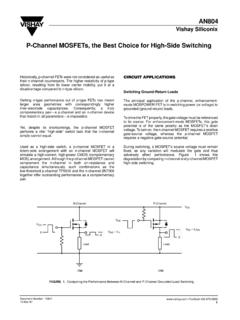
1 LT115811158fb TYPICAL APPLICATION DESCRIPTIONHalf Bridge N-ChannelPower MOSFET DriverA single input pin on the LT 1158 synchronously controls two N-Channel Power MOSFETs in a totem pole confi gura-tion. Unique adaptive protection against shoot-through currents eliminates all matching requirements for the two MOSFETs. This greatly eases the design of high effi ciency motor control and switching regulator continuous current limit loop in the LT1158 regulates short-circuit current in the top Power MOSFET . Higher start-up currents are allowed as long as the MOSFET VDS does not exceed By returning the FAULT output to the enable input, the LT1158 will automatically shut down in the event of a fault and retry when an internal pull-up current has recharged the enable on-chip charge pump is switched in when needed to turn on the top N-Channel MOSFET continuously.
2 Special circuitry ensures that the top side gate drive is safely maintained in the transition between PWM and DC opera-tion. The gate-to-source voltages are internally limited to when operating at higher supply , LT, LTC and LTM are registered trademarks of Linear Technology Corporation. All other trademarks are the property of their respective owners. Protected by Patents including and Bottom Gate Waveforms FEATURES APPLICATIONSn Drives Gate of Top side MOSFET Above V+n Operates at Supply Voltages from 5V to 30Vn 150ns Transition Times Driving 3000pFn Over 500mA Peak Driver Currentn Adaptive Non-Overlap Gate Drivesn Continuous Current Limit Protectionn Auto Shutdown and Retry Capabilityn Internal Charge Pump for DC Operationn Built-In Gate Voltage Protectionn Compatible with Current-Sensing MOSFETsn TTL/CMOS Input Levelsn Fault Output Indicationn PWM of High Current Inductive Loadsn Half Bridge and Full Bridge Motor Controln Synchronous Step-Down Switching Regulatorsn
3 Three-Phase Brushless Motor Driven High Current Transducer Driversn Battery-Operated Logic-Level MOSFETs+ 500 FIRFZ34 IRFZ3424V1N414810 F1 FPWM0Hz TO100kHzBOOSTBOOST DRT GATE DRT GATE FBT SOURCESENSE+SENSE B GATE DRB GATE FBGNDV+V+INPUTENABLEFAULTBIASLT1158 LOADLT1158 TA01+++VIN = 24 VRL = 12 1158 TA02LT115821158fb ABSOLUTE MAXIMUM RATINGSS upply Voltage (Pins 2, 10) ..36 VBoost Voltage (Pin 16) ..56 VContinuous Output Currents (Pins 1, 9, 15) ..100mASense Voltages (Pins 11, 12) .. 5V to V+ + 5 VTop Source Voltage (Pin 13) .. 5V to V+ + 5 VBoost to Source Voltage (V16 V13) .. to 20V(Note 1)12345678 TOP VIEWN PACKAGE16-LEAD PLASTIC DIP161514131211109 BOOST DRV+BIASENABLEFAULTINPUTGNDB GATE FBBOOSTT GATE DRT GATE FBT SOURCESENSE+SENSE V+B GATE DR JA = 70 C/W12345678 TOP VIEWSW PACKAGE16-LEAD PLASTIC (WIDE) SO161514131211109 BOOST DRV+BIASENABLEFAULTINPUTGNDB GATE FBBOOSTT GATE DRT GATE FBT SOURCESENSE+SENSE V+B GATE DR JA = 110 C/W PIN CONFIGURATIONORDER INFORMATIONLEAD FREE FINISHTAPE AND REELPART MARKING*PACKAGE DESCRIPTIONTEMPERATURE RANGELT1158CN#PBFLT1158CN#TRPBF16-Lead Plastic DIP0 C to 70 CLT1158IN#PBFLT1158IN#TRPBF16-Lead Plastic DIP 40 C to 85 CLT1158 CSW#PBFLT1158 CSW#TRPBF16-Lead Plastic (Wide)
4 SO0 C to 70 CLT1158 ISW#PBFLT1158 ISW#TRPBF16-Lead Plastic (Wide) SO 40 C to 85 CLEAD BASED FINISHTAPE AND REELPART MARKING*PACKAGE DESCRIPTIONTEMPERATURE RANGELT1158 CNLT1158CN#TR16-Lead Plastic DIP0 C to 70 CLT1158 INLT1158IN#TR16-Lead Plastic DIP 40 C to 85 CLT1158 CSWLT1158 CSW#TR16-Lead Plastic (Wide) SO0 C to 70 CLT1158 ISWLT1158 ISW#TR16-Lead Plastic (Wide) SO 40 C to 85 CConsult LTC Marketing for parts specifi ed with wider operating temperature ranges. *The temperature grade is identifi ed by a label on the shipping more information on lead free part marking, go to: For more information on tape and reel specifi cations, go to: Temperature RangeLT1158C.
5 0 C to 70 CLT1158I .. 40 C to 85 CJunction Temperature (Note 2)LT1158C .. 125 CLT1158I .. 150 CStorage Temperature Range .. 65 C to 150 CLead Temperature (Soldering, 10 sec.) .. 300 CLT115831158fb ELECTRICAL CHARACTERISTICSNote 1: Stresses beyond those listed under Absolute Maximum Ratings may cause permanent damage to the device. Exposure to any Absolute Maximum Rating condition for extended periods may affect device reliability and 2: TJ is calculated from the ambient temperature TA and Power dissipation PD according to the following formulas:LT1158IN, LT1158CN: TJ = TA + (PD 70 C/W) LT1158 ISW, LT1158 CSW: TJ = TA + (PD 110 C/W) The l denotes the specifi cations which apply over the full operating temperature range, otherwise specifi cations are at TA = 25 C.
6 Test Circuit, V+ = V16 = 12V, V11 = V12 = V13 = 0V, Pins 1 and 4 open, Gate Feedback pins connected to Gate Drive pins unless otherwise specifi + I10DC Supply Current (Note 2)V+ = 30V, V16 = 15V, V4 = + = 30V, V16 = 15V, V6 = + = 30V, V16 = 15V, V6 = CurrentV+ = V13 = 30V, V16 = 45V, V6 = CurrentV6 = 5Vl515515 AV4 Enable Low ThresholdV6 = , Monitor V4 Enable HysteresisV6 = , Monitor Pullup CurrentV4 = 0Vl152535152535 AV15 Charge Pump VoltageV+ = 5V, V6 = 2V, Pin 16 open, V13 5VV+ = 30V, V6 = 2V, Pin16 open, V13 30 Vll940114347940114347 VVV9 Bottom Gate ON VoltageV+ = V16 = 18V, V6 = Drive VoltageV+ = V16 = 18V, V6 = , 100mA Pulsed V13 Top Turn-Off ThresholdV+ = V16 = 5V, V6 = Turn-Off ThresholdV+ = V16 = 5V, V6 = Output LeakageV+ = 30V, V16 = 15V.
7 V6 = AV5 Fault Output SaturationV+ = 30V, V16 = 15V, V6 = 2V, I5 = V11 Fault Conduction ThresholdV+ = 30V, V16 = 15V, V6 = 2V, I5 = 100 A9011013085110135mVV12 V11 Current Limit ThresholdV+ = 30V, V16 = 15V, V6 = 2V, Closed Loopl130120150170180120120150180180mVmVV 12 V11 Current Limit Inhibit VDS ThresholdV+ = V12 = 12V, V6 = 2V, Decrease V11 Until V15 Goes Gate Rise TimePin 6 (+) Transition, Meas. V15 V13 (Note 4)l130250130250nstDTop Gate Turn-Off DelayPin 6 ( ) Transition, Meas. V15 V13 (Note 4)l350550350550nstFTop Gate Fall TimePin 6 ( ) Transition, Meas. V15 V13 (Note 4)l120250120250nstRBottom Gate Rise TimePin 6 ( ) Transition, Meas.
8 V9 (Note 4)l130250130250nstDBottom Gate Turn-Off DelayPin 6 (+) Transition, Meas. V9 (Note 4)l200400200400nstFBottom Gate Fall TimePin 6 (+) Transition, Meas. V9 (Note 4)l100200100200nsNote 3: Dynamic supply current is higher due to the gate charge being delivered at the switching frequency. See typical performance characteristics and applications 4: Gate rise times are measured from 2V to 10V, delay times are measured from the input transition to when the gate voltage has decreased to 10V, and fall times are measured from 10V to TYPICAL PERFORMANCE CHARACTERISTICSD ynamic Supply CurrentCharge Pump Output VoltageInput ThresholdsEnable ThresholdsFault Conduction ThresholdCurrent Limit ThresholdDC Supply CurrentDC Supply CurrentDynamic Supply Current (V+)SUPPLY VOLTAGE (V)08101230LT1158 G01641020402014I2 + I10 + I16 ENABLE LOWSUPPLY CURRENT (mA)5152535 INPUT LOWINPUT HIGHV13 = 0VV13 = V+TEMPERATURE ( C) 50810142575LT1158 G0264 250501001252012 SUPPLY CURRENT (mA)
9 I2 + I10 + I16V+ = 12 VINPUT HIGHINPUT LOWENABLE LOWINPUT FREQUENCY (kHz)10 SUPPLY CURRENT (mA)51015203010100LT1158 G032550% DUTY CYCLECGATE = 3000pFV+ = 24VV+ = 6VV+ = 12 VINPUT FREQUENCY (kHz)10 SUPPLY CURRENT (mA)51015204010100LT1158 G04253035 CGATE = 10000pF50% DUTY CYCLEV+ = 12 VCGATE = 1000pFCGATE = 3000pFSUPPLY VOLTAGE (V)00 TOP GATE VOLTAGE (V)51520255035102025LT1158 G051040453051530354010 A LOADNO LOADSUPPLY VOLTAGE (V) THRESHOLD VOLTAGE (V) (HIGH)V(LOW) 40 C+25 C+85 C 40 C+25 C+85 CSUPPLY VOLTAGE (V) (HIGH)V(LOW) 40 C+25 C+85 C 40 C+25 C+85 CENABLE THRESHOLD VOLTAGE (V)5152535 SUPPLY VOLTAGE (V)060 FAULT CONDUCTION THRESHOLD (mV)7090100110160130102025LT1158 G0880140150120515303540V11 = 0V 40 C+25 C+85 CSUPPLY VOLTAGE (V)0100 CURRENT LIMIT THRESHOLD (mV)110130140150200170102025LT1158 G09120180190160515303540 CLOSED LOOP+85 C 40 C+25 CLT115851158fbTYPICAL PERFORMANCE CHARACTERISTICSTop Gate Rise TimeTop Gate Fall TimeTransition Times vs RGateCurrent Limit Inhibit VDS ThresholdBottom Gate Rise TimeBottom Gate Fall TimeSUPPLY VOLTAGE (V) LIMIT INHIBIT THRESHOLD (V) V11 40 C+25 C+85 CSUPPLY VOLTAGE (V)0 BOTTOM GATE RISE TIME (ns)20025030040LT1158 G11150100010203050400350 CGATE = 10000pFCGATE = 1000pFCGATE = 3000pF5152535 SUPPLY VOLTAGE (V)0 BOTTOM GATE FALL TIME (ns)
10 20025030040LT1158 G12150100010203050400350 CGATE = 10000pFCGATE = 1000pFCGATE = 3000pF5152535 SUPPLY VOLTAGE (V)0 TOP GATE RISE TIME (ns)20025030040LT1158 G13150100010203050400350 CGATE = 10000pFCGATE = 1000pFCGATE = 3000pF5152535 SUPPLY VOLTAGE (V)0 TOP GATE FALL TIME (ns)20025030040LT1158 G14150100010203050400350 CGATE = 10000pFCGATE = 1000pFCGATE = 3000pF5152535 GATE RESISTANCE ( )0 TRANSITION TIMES (ns)60080080LT1158 G154002000204060100700500300100103050709 0V+ = 12 VCGATE = 3000pFRISE TIMEFALL TIMELT115861158fb PIN FUNCTIONSBOOST DR (Pin 1): Recharges and clamps the bootstrap capacitor to higher than pin 13 via an external + (Pin 2): Main supply pin; must be closely decoupled to the ground pin (Pin 3): Decouple point for the internal bias generator.