Transcription of LT1302 - Micropower High Output Current Step …
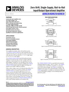
1 1LT13 0 2/ LT13 0 2 - 5 MicropowerHigh Output CurrentStep-Up Adjustable andFixed 5V DC/DC ConvertersFigure 1. 2-Cell to 5V/600mA DC/DC ConverterSFEATUREDUESCRIPTIOn5V at 600mA or 12V at 120mA from 2-Cell Supplyn200 A Quiescent CurrentnLogic Controlled Shutdown to 15 AnLow VCESAT Switch: 310mV at 2A TypicalnBurst ModeTM Operation at Light LoadnCurrent Mode Operation for ExcellentLine and Load Transient ResponsenAvailable in 8-Lead SO or PDIPnOperates with Supply Voltage as Low as 2 VThe LT 1302/ LT1302 -5 are Micropower step -up DC/DCconverters that maintain high efficiency over a widerange of Output Current . They operate from a supplyvoltage as low as 2V and feature automatic shiftingbetween Burst Mode operation at light load, and currentmode operation at heavy internal low loss NPN power switch can handlecurrent in excess of 2A and switch at frequencies up to400kHz.
2 Quiescent Current is just 200 A and can befurther reduced to 15 A in in 8-pin PDIP or 8-pin SO packaging, the LT1302 / LT1302 -5 have the highest switch Current rating of anysimilarly packaged switching regulators presently on , LTC and LT are registered trademarks of Linear Technology Mode is a trademark of Linear Technology and Palmtop ComputersnPortable InstrumentsnPersonal Digital AssistantsnCellular TelephonesnFlash MemoryUAOPPLICATITYPICAL+NCC3 FSHUTDOWNVINITVCSWPGNDSHDNSENSEGND2RC 20kCC FC1 100 FD1+C2 100 FL1 10 H2 CELLSLT1302 F01C1 = C2 = SANYO OS-CON L1 = COILTRONICS CTX10-3 COILCRAFT DO3316-103 Output 5V 600mA 1876534D1 = MOTOROLA MBRS130LT3 LT1302 -5 LOAD Current (mA)178 EFFICIENCY (%)80828486101001000LT1302 TA02767472708890 VIN = 3 VVIN = = 2V2-Cell to 5V Converter Efficiency2LT13 0 2/ LT13 0 2 - 5 AUGWAWUWARBSOLUTEXITISWUUPACKAGE/ORDER I FOR ATIOVIN Voltage.
3 10 VSW Voltage .. 25 VFB Voltage .. 10 VSHDN Voltage .. 10 VVC Voltage .. 4 VIT Voltage .. 4 VMaximum Power Dissipation .. 700mWOperating Temperature Range .. 0 C to 70 CStorage Temperature Range .. 65 C to 150 CLead Temperature (Soldering, 10 sec) .. 300 CConsult factory for Industrial and Military grade PARTNUMBERLT1302CN8LT1302CS8LT1302CN8-5L T1302CS8-5S8 PART MARKING130213025 SYMBOLPARAMETERCONDITIONSMINTYPMAXUNITSI QQ uiescent CurrentVSHDN = , VFB = AVSHDN = AVINI nput Voltage Voltage ( LT1302 )VC = Pin Bias Current ( LT1302 )VFB = 1V100nAOutput Sense Voltage ( LT1302 -5)VC = Ripple Voltage ( LT1302 -5)VC = Pin Resistance to Ground ( LT1302 -5)420k VOSO ffset VoltageSee Block Diagram15mVComparator Hysteresis(Note 1)5mVOscillator FrequencyCurrent Limit Not Asserted (Note 2)
4 175220265kHzl160310kHZDCM aximum Duty Cycle758695%tONSwitch On TimeCurrent Limit Not stOFFS witch Off sOutput Line Regulation2 < VIN < VVCESATS witch Saturation VoltageISW = 2A310400mVl475mVSwitch Leakage CurrentVSW = 5V, Switch ASwitch Current LimitVC = (Burst Mode Operation)1 AVC = (Full Power) (Note 3) Amplifier Voltage VC , VC/ VFB5075V/ VVSHDNHS hutdown Pin Pin Pin Bias CurrentVSHDN = 5Vl820 AVSHDN = 2V3 AVSHDN = AIT Pin Resistance to TA = 25 C, VIN = , unless otherwise CCHARA TERISTICSCDThe l denotes specifications which apply over the 0 C to 70 Ctemperature 1: Hysteresis is specified at DC. Output ripple depends on capacitorsize and 2: The LT1302 operates in a variable frequency mode.
5 Switchingfrequency depends on load inductance and operating conditions and maybe above specified 3: Minimum switch Current 100% tested. Maximum switch currentguaranteed by 2 3 48 7 6 5 TOP VIEWGND VC SHDN (SENSE*)FBPGND SW VIN ITN8 PACKAGE 8-LEAD PDIPS8 PACKAGE 8-LEAD PLASTIC SO*FIXED VERSION PINS 1 AND 8 ARE INTERNALLY CONNECTED IN SOIC PACKAGETJMAX = 125 C, JA = 100 C/W (N8)TJMAX = 125 C, JA = 80 C/W (S8)3LT13 0 2/ LT13 0 2 - 5 TYPICAL PERFORMANCE CHARACTERISTICS UWTEMPERATURE ( C) 50 SATURATION VOLTAGE (mV)400 350 300 250 200 150 100 25025501302 G0375100 ISW = 2 ATEMPERATURE ( C) 50 FEEDBACK VOLTAGE (V) 25025501302 G0475100 SUPPLY VOLTAGE (V) Current ( A)500 450 400 350 300 250 200 150 100 50 01302 G01TA = 25 CNo-Load Quiescent CurrentCircuit of Figure 1 TEMPERATURE ( C) 50 SENSE RESISTANCE (k )
6 600 500 400 300 200 100 0 25025501302 G0575100 TEMPERATURE ( C) 50 QUIESCENT Current ( A)300 250 200 150 100 50 0 25025501302 G0675100 VIN = SWITCH OFFTEMPERATURE ( C) 50 OFFSET VOLTAGE (mV)30 25 20 15 10 5 0 25025501302 G0775100 TEMPERATURE ( C) 50 Output VOLTAGE (V) 25025501302 G0875100 TEMPERATURE ( C) 50ON-TIME ( s) 25025501302 G0975100 SWITCH Current (A)0 VCESAT (V)600 500 400 300 200 100 012 341302 G02TA = 25 CSwitch Saturation VoltageSwitch Saturation VoltageLT1302 Feedback VoltageLT1302-5 Sense Pin ResistanceQuiescent CurrentError Amplifier Offset VoltageLT1302-5 Output VoltageMaximum On-Time4LT13 0 2/ LT13 0 2 - 5 TYPICAL PERFORMANCE CHARACTERISTICS UWTEMPERATURE ( C) 50 DUTY CYCLE (%)100 90 80 70 60 50 25025501302 G1075100 TEMPERATURE ( C) 50 FREQUENCY (kHz)300 275 250 225 200 175 150 25025501302 G1175100 SHUTDOWN VOLTAGE (V)0 SHUTDOWN Current ( A) 20 18 16 14 12 10 8 6 4 2 0451302 G12132678TA = 25 CGND (Pin 1): Signal Ground.
7 Feedback resistor and Fceramic bypass capacitor from VIN should be connecteddirectly to this (Pin 2): Frequency Compensation Pin. Connect seriesRC to GND. Keep trace (Pin 3): Shutdown. Pull high to effect shutdown; tieto ground for normal (Pin 4): Feedback/Sense. On the LT1302 thispin connects to CMP1 input. On the LT1302 -5 this pinconnects to the Output resistor FU CTIO S UUUIT (Pin 5): Normally left floating. Addition of a resistorto GND forces the LT1302 into Current mode at light drops at light load but increases at mediumloads. See Applications Information (Pin 6): Supply Pin. Must be bypassed with: (1) a Fceramic to GND, and (2) a large value electrolytic to VIN is greater than 5V, a low value resistor (2 to10 ) is recommended to isolate the VIN pin from inputsupply Duty CycleOscillator FrequencyShutdown Pin Bias CurrentLT1302-5 Output Voltage vsLoad CurrentLOAD Current (A)0 Output VOLTAGE (V) G13 = = 3 VVIN = 4 VMaximum Output Power*Boost ModeINPUT VOLTAGE (V)0 Output POWER (W)20 16 12 8 4 081302 G1424* APPROXIMATE6105LT13 0 2/ LT13 0 2 - 5PI FU CTIO S UUUSW (Pin 7): Switch Pin.
8 Connect inductor and diode layout short and (Pin 8): Power Ground. Pins 8 and 1 should beconnected under the package. In the SO package, pins 1and 8 are thermally connected to the die. One square inchof PCB copper provides an adequate heat sink for 2. LT1302 Block Diagram1302 F02 + + +VOS 15mVR2C5 100pF36mVCMP1 OFFVIN2 AENABLEA2 VINC2 FC1 VINL1 SWPGNDITVCR3 22kC4 FGNDSHDNSHUTDOWNFBERROR AMPLIFIERHYSTERETIC REFERENCE220kHz OSCILLATOR300 R5 730 VINBIASR16+C3D1 VOUT+Q4 160XA3Q1Q2Q5 BLOCK DIAGRA SMW6LT13 0 2/ LT13 0 2 - 5 BLOCK DIAGRA SMWThe LT1302 s operation can best be understood byexamining the block diagram in Figure 2. The LT1302operates in one of two modes, depending on load.
9 Withlight loads, comparator CMP1 controls the Output ; withheavy loads, control is passed to error amplifier Mode operation consists of monitoring the FB pinvoltage with hysteretic comparator CMP1. When the FBvoltage, related to the Output voltage by external attenu-ator R1 and R2, falls below the reference voltage,the oscillator is enabled. Switch Q4 alternately turns on,causing Current buildup in inductor L1, then turns off,allowing the built-up Current to flow into Output capaci-tor C3 via D1. As the Output voltage increases, so doesthe FB voltage; when it exceeds the reference plusOPERATIOUCMP1 s hysteresis (about 5mV) CMP1 turns the oscilla-tor off. In this mode, peak switch Current is limited toapproximately 1A by A2, Q2, and Q3.
10 Q2 s Current , set at34 A, flows through R5, causing A2 s negative input tobe 25mV lower than VIN. This node must fall more than36mV below VIN for A2 to trip and turn off the remaining 11mV is generated by Q3 s Current flow-ing through R4. Emitter-area scaling sets Q3 s collectorcurrent to of switch Q4 s Current . When Q4 scurrent is 1A, Q3 s Current is , creating an 11mVdrop across R4 which, added to R5 s 25mV drop, isenough to trip the Output load is increased to the point where the1A peak Current cannot support the Output voltage,1302 F03 + + +VOS 15mV36mVCMP1 OFFVIN2 AENABLEA2 VINSWPGNDITVCGNDSHDNSHUTDOWNSENSEERROR AMPLIFIERHYSTERETIC REFERENCE220kHz OSCILLATOR300 R5 730 VINBIASR1 315kR2 105k6Q4 160XA3Q1Q2Q5 Figure 3.
