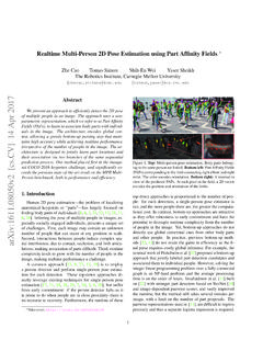
Transcription of LT1611 - Inverting 1.4MHz Switching Regulator in 5 …
1 LT1611 . Inverting Switching Regulator in SOT-23. U. FEATURES DESCRIPTIO. Very Low Noise: 1mVP P Output Ripple The LT 1611 is the industry's first Inverting 5-lead SOT-23. 5V at 150mA from a 5V Input current mode DC/DC converter. Intended for use in small, Better Regulation Than a Charge Pump low power applications, it operates from an input voltage Effective Output Impedance: as low as and switches at , allowing the use Uses Tiny Capacitors and Inductors of tiny, low cost capacitors and inductors 2mm or less in Internally Compensated height. Its small size and high Switching frequency enable Fixed Frequency Operation the complete DC/DC converter function to consume less Low Shutdown Current: <1 A than square inches of PC board area. Capable of Low VCESAT Switch: 300mV at 300mA generating 5V at 150mA from a 5V supply or 5V at Tiny 5-Lead SOT-23 Package 100mA from a 3V supply, the LT1611 replaces nonregulated charge pump solutions in many applications.
2 U. APPLICATIO S The LT1611 operates in a dual inductor Inverting topology which filters the input side as well as the output side of the MR Head Bias DC/DC converter. Fixed frequency Switching ensures a Digital Camera CCD Bias clean output free from low frequency noise typically present LCD Bias with charge pump solutions. No load quiescent current of GaAs FET Bias the LT1611 is 3mA, while in shutdown quiescent current Positive-to-Negative Conversion drops to A. The 36V switch allows VIN to VOUT. differential of up to 33V. The LT1611 is available in the 5-lead SOT-23 package. , LTC and LT are registered trademarks of Linear Technology Corporation. U. TYPICAL APPLICATIO. C2. L1A. 1 F. L1B Transient Response 22 H 22 H. VIN. 5V. D1. VIN SW VOUT. 5V. SHDN R1 150mA. + C1 LT1611 1200pF VOUT.
3 20mV/DIV. 22 F NFB C3. 22 F AC COUPLED. GND R2. 10k 150mA. LOAD CURRENT. 50mA. C1: AVX TAJB226M010 1611 TA01. C2: TAIYO YUDEN LMK212BJ105MG 100 s/DIV 1611 F10. C3: TAIYO YUDEN JMK325BJ226MM (1210 SIZE). D1: MBR0520. L1: SUMIDA CLS62-220 OR 2 MURATA LQH3C220 (UNCOUPLED). Figure 1. 5V to 5V, 150mA Low Noise Inverting DC/DC Converter 1. LT1611 . W W W U U W U. ABSOLUTE MAXIMUM RATINGS PACKAGE/ORDER INFORMATION. (Note 1). VIN Voltage .. 10V ORDER PART. TOP VIEW NUMBER. SW Voltage .. to 36V. SW 1 5 VIN. NFB Voltage .. 3V GND 2 LT1611CS5. Current into NFB Pin .. 1mA NFB 3 4 SHDN. SHDN Voltage .. 10V. S5 PACKAGE. Maximum Junction Temperature .. 125 C 5-LEAD PLASTIC SOT-23 S5 PART MARKING. Operating Temperature Range Commercial .. 0 C to 70 C TJMAX = 125 C, JA = 256 C/W LTES. Extended Commercial (Note 2).
4 40 C to 85 C. Storage Temperature Range .. 65 C to 150 C Consult factory for Industrial and Military grade parts. Lead Temperature (Soldering, 10 sec).. 300 C. ELECTRICAL CHARACTERISTICS The denotes the specifications which apply over the full operating temperature range, otherwise specifications are at TA = 25 C. VIN = , VSHDN = VIN unless otherwise noted. PARAMETER CONDITIONS MIN TYP MAX UNITS. Minimum Operating Voltage V. Maximum Operating Voltage 10 V. NFB Pin Bias Current VNFB = A. Feedback Voltage V. Quiescent Current VSHDN = , Not Switching 3 mA. Quiescent Current in Shutdown VSHDN = 0V, VIN = 2V A. VSHDN = 0V, VIN = 5V A. Reference Line Regulation VIN 10V %/V. Switching Frequency MHz Maximum Duty Cycle 82 86 %. Switch Current Limit (Note 3) 550 800 mA. Switch VCESAT ISW = 300mA 300 350 mV.
5 Switch Leakage Current VSW = 5V 1 A. SHDN Input Voltage High 1 V. SHDN Input Voltage Low V. SHDN Pin Bias Current VSHDN = 3V 25 50 A. VSHDN = 0V 0 A. Note 1: Absolute Maximum Ratings are those values beyond which the life Note 3: Current limit guaranteed by design and/or correlation to static test. of a device may be impaired. Slope compensation reduces current limit at higher duty cycle. Note 2: C grade device specifications are guaranteed over the 0 C to 70 C. temperature range. In addition, C grade device specifications are assured over the 40 C to 85 C temperature range by design or correlation, but are not production tested. 2. LT1611 . U W. TYPICAL PERFOR A CE CHARACTERISTICS. NFB Pin Bias Current vs Efficiency, VOUT = 5V VNFB vs Temperature Temperature 85 6. 80 5. NFB PIN BIAS CURRENT ( A).
6 VIN = 5V. 75 4. EFFICIENCY (%). 70 VIN = 3V. VNFB (V). 3. 65 2. 60 55 1. 50 0. 0 25 50 75 100 125 150 50 25 0 25 50 75 100 50 25 0 25 50 75 100. LOAD CURRENT (mA) TEMPERATURE ( C) TEMPERATURE ( C). 1611 G01 1611 G02 1611 G03. Switch VCESAT vs Switch Current SHDN Pin Bias Current vs VSHDN Switch Current Limit vs Duty Cycle 700 50 900. TA = 25 C TA = 25 C. 600 800. SHDN PIN BIAS CURRENT ( A). SWITCH CURRENT LIMIT (mA). 40 700. 500. 600. VCESAT (mV). 400 30. 500. 300 400. 20. 300. 200. 10 200. 100. 100. 0 0 0. 0 100 200 300 400 500 600 700 0 1 2 3 4 5 10 20 30 40 50 60 70 80. SWITCH CURRENT (mA) SHDN PIN VOLTAGE (V) DUTY CYCLE (%). 1611 G04 1611 G05 1611 G06. Oscillator Frequency vs No-Load Operating Quiescent Switch Current Limit vs Temperature Current vs Temperature* Temperature (Duty Cycle = 30%).
7 900. VIN = 5V 800. Switching FREQUENCY (MHz). SWITCH CURRENT LIMIT (mA). 700. OPERATING CURRENT (mA). VIN = 600. 500. 400. 300. 200. 100. 0 0. 50 25 0 25 50 75 100 50 25 0 25 50 75 100 50 25 0 25 50 75 100. TEMPERATURE ( C) TEMPERATURE ( C) TEMPERATURE ( C). 1611 G07 1611 G08 1611 G09. * Includes bias current through R1, R2 and Schottky leakage current at T 75 C. 3. LT1611 . U U U. PIN FUNCTIONS. SW (Pin 1): Switch Pin. Minimize trace area at this pin to VOUT keep EMI down. R1 =.. GND (Pin 2): Ground. Tie directly to local ground plane. + 10 6 . R2 . NFB (Pin 3): Negative Feedback Pin. Minimize trace area. SHDN (Pin 4): Shutdown Pin. Tie to 1V or more to enable Reference voltage is Connect resistive divider tap device. Ground to shut the device down. here. The suggested value for R2 is 10k.
8 Set R1 and R2. according to: VIN (Pin 5): Input Supply Pin. Must be locally bypassed. W. BLOCK DIAGRAM. VIN 5 VIN. R5 R6. 40k 40k 1 SW. + COMPARATOR. A1 . gm DRIVER. FF. A2 R Q Q3. RC + S. Q1 Q2. RAMP. GENERATOR . x10. CC +. VOUT R3. A=3 . 30k R1.. CPL OSCILLATOR. (EXTERNAL) R4. (OPTIONAL). 140k NFB SHDN. R2 3 NFB 4 SHUTDOWN 2 GND. (EXTERNAL) 1611 BD. Figure 2. U. OPERATIO. The LT1611 combines a current mode, fixed frequency flop and turning off the switch. Output voltage decreases PWM architecture with a reference to directly (the magnitude increases) as switch current is increased. regulate negative outputs. Operation can be best under- The output, attenuated by external resistor divider R1 and stood by referring to the block diagram of Figure 2. Q1 and R2, appears at the NFB pin, closing the overall loop.
9 Q2 form a bandgap reference core whose loop is closed Frequency compensation is provided internally by RC and around the output of the converter. The driven reference CC. Transient response can be optimized by the addition of point is the lower end of resistor R4, which normally sits a phase lead capacitor, CPL, in parallel with R1 in applica- at a voltage of As the load current changes, the tions where large value or low ESR output capacitors are NFB pin voltage also changes slightly, driving the output used. of gm amplifier A1. Switch current is regulated directly on As load current is decreased, the switch turns on for a a cycle-to-cycle basis by A1's output. The flip-flop is set at shorter period each cycle. If the load current is further the beginning of each cycle, turning on the switch.
10 When decreased, the converter will skip cycles to maintain the summation of a signal representing switch current and output voltage regulation. a ramp generator (introduced to avoid subharmonic oscil- lations at duty factors greater than 50%) exceeds the VC The LT1611 can work in either of two topologies. The signal, comparator A2 changes stage, resetting the flip- simpler topology appends a capacitive level shift to a 4. LT1611 . U. OPERATIO. boost converter, generating a negative output voltage, When Q1 turns off during the second phase of Switching , which is directly regulated. The circuit schematic is de- the SW node voltage abruptly increases to (VIN + |VOUT|). tailed in Figure 3. Only one inductor is required, and the The SWX node voltage increases to VD (about 350mV). two diodes can be in a single SOT-23 package.