Transcription of LT8302/LT8302-3 (Rev. G) - Analog Devices
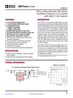
1 LT8302/LT8302-31 Rev. GFor more information FeedbackTYPICAL APPLICATION FEATURESDESCRIPTION42 VIN Micropower No- opto isolated Flyback Converter with 65 SwitchThe LT 8302/LT8302-3 is a monolithic micropower iso-lated flyback converter. By sampling the isolated output voltage directly from the primary-side flyback waveform, the part requires no third winding or opto -isolator for regulation. The output voltage is programmed with two external resistors and a third optional temperature com-pensation resistor. Boundary mode operation provides a small magnetic solution with excellent load regulation. Low ripple Burst Mode operation maintains high efficiency at light load while minimizing the output voltage ripple. A , 65V DMOS power switch is integrated along with all the high voltage circuitry and control logic into a thermally enhanced 8-lead SO LT8302/LT8302-3 operates from an input voltage range of 3V to 42V and delivers up to 18W of isolated output power.
2 The high level of integration and the use of boundary and low ripple burst modes result in a simple to use, low component count, and high efficiency application solution for isolated power delivery. 3V to 32 VIN/5 VOUT isolated Flyback ConverterAPPLICATIONS n3V to 42V Input Voltage Range , 65V Internal DMOS Power Switch nLow Quiescent Current: n106 A in Sleep Mode n380 A in Active Mode nQuasi-Resonant Boundary Mode Operation at Heavy Load nLow Ripple Burst Mode Operation at Light Load nMinimum Load < (Typ) of Full Output nNo Transformer Third Winding or opto -Isolator Required for Output Voltage Regulation nAccurate EN/UVLO Threshold and Hysteresis nInternal Compensation and Soft-Start nTemperature Compensation for Output Diode nOutput Short-Circuit Protection nThermally Enhanced 8-Lead SO Package nAEC-Q100 Qualified for Automotive Applications nIsolated Automotive, Industrial, Medical Power Supplies nIsolated Auxiliary/Housekeeping Power SuppliesEfficiency vs Load CurrentVINLT8302/LT8302-3SW9 HVIN3V TO 32V3.
3 11 HRFBRREFEN/UVLO470pF10 F1 F220 F10mA TO (VIN = 5V)10mA TO (VIN = 12V)10mA TO (VIN = 24V)VOUT 39 154k 115k10k8302 TA01aGNDINTVCCTCVOUT+5 VLOAD CURRENT (A)0 EFFICIENCY (%) = 5 VVIN = 12 VVIN = 24 VAll registered trademarks and trademarks are the property of their respective owners. Protected by patents, including 5438499, 7463497, GFor more information CONFIGURATIONABSOLUTE MAXIMUM RATINGSSW (Note 2) ..65 VVIN ..42 VEN/UVLO ..VINRFB ..VIN to VINC urrent Into RFB ..200 AINTVCC, RREF, TC ..4 VOperating Junction Temperature Range (Notes 3, 4) LT8 302E, LT8 302E-3 .. 40 C to 125 C LT8 302I, LT8 302I-3 .. 40 C to 125 C LT8 302J, LT8 302J-3 .. 40 C to 150 C LT8 302H, LT8 302H-3 .. 40 C to 150 C LT8 302MP .. 55 C to 150 CStorage Temperature Range .. 65 C to 150 CLead Temperature (Soldering, 10 sec) ..300 C (Note 1)LEAD FREE FINISHTAPE AND REELPART MARKING*PACKAGE DESCRIPTIONTEMPERATURE RANGELT8302ES8E#PBFLT8302ES8E#TRPBF83028 -Lead Plastic SO 40 C to 125 CLT8302IS8E#PBFLT8302IS8E#TRPBF83028-Lea d Plastic SO 40 C to 125 CLT8302JS8E#PBFLT8302JS8E#TRPBF83028-Lea d Plastic SO 40 C to 150 CLT8302HS8E#PBFLT8302HS8E#TRPBF83028-Lea d Plastic SO 40 C to 150 CLT8302 MPS8E#PBFLT8302 MPS8E#TRPBF83028-Lead Plastic SO 55 C to 150 CLT8302ES8E-3#PBFLT8302ES8E-3#TRPBF83023 8-Lead Plastic SO 40 C to 125 CLT8302IS8E-3#PBFLT8302IS8E-3#TRPBF83023 8-Lead Plastic SO 40 C to 125 CLT8302JS8E-3#PBFLT8302JS8E-3#TRPBF83023 8-Lead Plastic SO 40 C to 150 CLT8302HS8E-3#PBFLT8302HS8E-3#TRPBF83023 8-Lead Plastic SO 40 C to 150 CAUTOMOTIVE PRODUCTS**LT8302ES8E#WPBFLT8302ES8E#WTRP BF83028-Lead Plastic SO 40 C to 125 CLT8302IS8E#WPBFLT8302IS8E#WTRPBF83028-L ead Plastic SO 40 C to 125 CLT8302JS8E#WPBFLT8302JS8E#WTRPBF83028-L ead Plastic SO 40 C to 150 CLT8302HS8E#WPBFLT8302HS8E#WTRPBF83028-L ead Plastic SO 40 C to 150
4 CLT8302ES8E-3#WPBFLT8302ES8E-3#WTRPBF830 238-Lead Plastic SO 40 C to 125 CLT8302IS8E-3#WPBFLT8302IS8E-3#WTRPBF830 238-Lead Plastic SO 40 C to 125 CLT8302JS8E-3#WPBFLT8302JS8E-3#WTRPBF830 238-Lead Plastic SO 40 C to 150 CLT8302HS8E-3#WPBFLT8302HS8E-3#WTRPBF830 238-Lead Plastic SO 40 C to 150 CContact the factory for parts specified with wider operating temperature ranges. *The temperature grade is identified by a label on the shipping and reel specifications. Some packages are available in 500 unit reels through designated sales channels with #TRMPBF suffix.**Versions of this part are available with controlled manufacturing to support the quality and reliability requirements of automotive applications. These models are designated with a #W suffix. Only the automotive grade products shown are available for use in automotive applications. Contact your local Analog Devices account representative for specific product ordering information and to obtain the specific Automotive Reliability reports for these INFORMATION12348765 TOP VIEWTCRREFRFBSWEN/UVLOINTVCCVINGNDS8E PACKAGE8-LEAD PLASTIC SO JA = 33 C/WEXPOSED PAD (PIN 9) IS GND, MUST BE SOLDERED TO PCB9 GNDLT8302/LT8302-33 Rev.
5 GFor more information CHARACTERISTICS The l denotes the specifications which apply over the full operating temperature range, otherwise specifications are at TA = 25 C. VIN = 5V, VEN/UVLO = VIN, CINTVCC = 1 F to GND, unless otherwise Voltage Rangel342 VIQVIN Quiescent CurrentVEN/UVLO = VEN/UVLO = Sleep Mode (Switch Off) Active Mode (Switch On) 53 106 3802 A A A AEN/UVLO Shutdown ThresholdFor Lowest Off Enable ThresholdFalling (E, I, H, MP Grades) Enable ThresholdFalling (J Grade Only) Enable Hysteresis14mVIHYSEN/UVLO Hysteresis CurrentVEN/UVLO = VEN/UVLO = VEN/UVLO = A A AVINTVCCINTVCC Regulation VoltageIINTVCC = 0mA to Current LimitVINTVCC = UVLO UVLO Hysteresis105mV(RFB VIN) VoltageIRFB = 75 A to 125 A 5050mVRREF Regulation Regulation Voltage Line Regulation3V VIN 42V Pin Pin CurrentVTC = (LT8302) VTC = (LT8302-3) VTC = 715 10 20018 13 A A AfMINM inimum Switching (MIN)Minimum Switch-On Time160nstOFF(MAX)Maximum Switch-Off TimeBackup Timer170 sISW(MAX)Maximum Switch Current (MIN)Minimum Switch Current (ON)
6 Switch On-ResistanceISW = ILKGS witch Leakage CurrentVSW = AtSSSoft-Start Timer11msNote 1: Stresses beyond those listed under Absolute Maximum Ratings may cause permanent damage to the device. Exposure to any Absolute Maximum Rating condition for extended periods may affect device reliability and 2: The SW pin is rated to 65V for transients. Depending on the leakage inductance voltage spike, operating waveforms of the SW pin should be derated to keep the flyback voltage spike below 65V as shown in Figure 3: The LT8302E/LT8302E-3 is guaranteed to meet performance specifications from 0 C to 125 C junction temperature. Specifications over the 40 C to 125 C operating junction temperature range are assured by design, characterization and correlation with statistical process controls. The LT8302I/LT8302I-3 is guaranteed over the full 40 C to 125 C operating junction temperature range. The LT8302J/LT8302J-3 and LT8302H/LT8302H-3 are guaranteed over the full 40 C to 150 C operating junction temperature range.
7 The LT8302MP is guaranteed over the full 55 C to 150 C operating junction temperature range. High junction temperatures degrade operating lifetimes. Operating lifetime is derated at junction temperature greater than 125 4: The LT8302/LT8302-3 includes overtemperature protection that is intended to protect the Devices during momentary overload conditions. Junction temperature will exceed 150 C when overtemperature protection is active. Continuous operation above the specified maximum operating junction temperature may impair device GFor more information PERFORMANCE CHARACTERISTICSB oundary Mode WaveformsDiscontinuous Mode WaveformsBurst Mode WaveformsVIN Shutdown CurrentVIN Quiescent Current, Sleep ModeVIN Quiescent Current, Active ModeOutput Load and Line RegulationOutput Temperature VariationSwitching Frequency vs Load CurrentTA = 25 C, unless otherwise ( C) 50 OUTPUT VOLTAGE (V) PAGE APPLICATIONVIN = 12 VIOUT = 1 ARTC = 115kRTC = OPENVSW20V/DIVVOUT50mV/DIV2 s/DIVFRONT PAGE APPLICATIONVIN = 12 VIOUT = 2A8302 G04 VSW20V/DIVVOUT50mV/DIV2 s/DIVFRONT PAGE APPLICATIONVIN = 12 VIOUT = G05 VSW20V/DIVVOUT50mV/DIV20 s/DIVFRONT PAGE APPLICATIONVIN = 12 VIOUT = 10mA8302 G06 VIN (V)0IQ ( A)6810408302 G0742010203050TJ = 150 CTJ = 25 CTJ = 55 CVIN (V)080IQ ( A)90100110120130140102030408302 G0850TJ = 150 CTJ = 55 CTJ = 25 CVIN (V)0IQ ( A)
8 380400420408302 G0936034032010203050TJ = 150 CTJ = 55 CTJ = 25 CLOAD CURRENT (A) (kHz) = 5 VVIN = 12 VVIN = 24 VFRONT PAGE APPLICATIONLOAD CURRENT (A)0 OUTPUT VOLTAGE (V) = 5 VVIN = 12 VVIN = 24 VLT8302/LT8302-35 Rev. GFor more information PERFORMANCE CHARACTERISTICSINTVCC Voltage vs VININTVCC UVLO Threshold (RFB-VIN) VoltageRREF Regulation VoltageRREF Line RegulationTC Pin VoltageEN/UVLO Enable ThresholdEN/UVLO Hysteresis CurrentINTVCC Voltage vs TemperatureTA = 25 C, unless otherwise ( C) 50 VEN/UVLO (V) ( C) 50 IHYST ( A)34525751508302 G11210 25050100125 TEMPERATURE ( C) (V) 252575125 IINTVCC = 0mAIINTVCC = 10mAVIN (V)5 VINTVCC (V) = 0mAIINTVCC = 10mATEMPERATURE ( C) (V) 252575125 FALLINGRISINGTEMPERATURE ( C) 50 VOLTAGE (mV)0201508302 G15 20 40050100 25257512540 1010 3030 IRFB = 125 AIRFB = 100 AIRFB = 75 ATEMPERATURE ( C) (V) 2525100125150 VIN (V)0 VRREF (V) ( C) 50 VTC (V) GFor more information Switching FrequencyMinimum Switch-On TimeMinimum Switch-Off TimeRDS(ON)Switch Current LimitMaximum Switching FrequencyTYPICAL PERFORMANCE CHARACTERISTICSTA = 25 C, unless otherwise ( C) 50 RESISTANCE (m )
9 12016020025751508302 G1980400 25050100125 TEMPERATURE ( C) 50 ISW (A)34525751508302 G20210 25050100125 MAXIMUM CURRENT LIMITMINIMUM CURRENT LIMITTEMPERATURE ( C) 50 FREQUENCY (kHz)30040050025751508302 G212001000 25050100125 TEMPERATURE ( C) 50 FREQUENCY (kHz)12162025751508302 G22840 25050100125 TEMPERATURE ( C) 500 TIME (ns)100200300400 25025508302 G2375100125150 TEMPERATURE ( C) 500 TIME (ns)100200300400 25025508302 G2475100125150LT8302/LT8302-37 Rev. GFor more information FUNCTIONSEN/UVLO (Pin 1): Enable/Undervoltage Lockout. The EN/UVLO pin is used to enable the LT8302/LT8302-3 . Pull the pin below to shut down the LT8302/LT8302-3 . This pin has an accurate threshold and can be used to program a VIN undervoltage lockout (UVLO) threshold using a resistor divider from VIN to ground. A A current hysteresis allows the programming of VIN UVLO hysteresis. If neither function is used, tie this pin directly to (Pin 2): Internal 3V Linear Regulator Output.
10 The INTVCC pin is supplied from VIN and powers the inter-nal control circuitry and gate driver. Do not overdrive the INTVCC pin with any external supply, such as a third wind-ing supply. Locally bypass this pin to ground with a mini-mum 1 F ceramic (Pin 3): Input Supply. The VIN pin supplies current to the internal circuitry and serves as a reference voltage for the feedback circuitry connected to the RFB pin. Locally bypass this pin to ground with a (Pin 4, Exposed Pad Pin 9): Ground. The exposed pad provides both electrical contact to ground and good thermal contact to the printed circuit board. Solder the exposed pad directly to the ground (Pin 5): Drain of the Internal DMOS Power Switch. Minimize trace area at this pin to reduce EMI and voltage (Pin 6): Input Pin for External Feedback Resistor. Connect a resistor from this pin to the transformer pri-mary SW pin. The ratio of the RFB resistor to the RREF resistor, times the internal voltage reference, determines the output voltage (plus the effect of any non-unity trans-former turns ratio).