Transcription of LT8357 (Rev. 0)
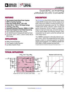
1 LT83571 Rev. 0 For more information FeedbackTYPICAL APPLICATION FEATURESDESCRIPTION60V 2 MHz Low-IQ Boost, SEPIC and Flyback ControllerThe LT 8357 is a wide input range, current mode, DC/DC controller which can be configured as a boost, SEPIC or flyback converter. The LT8357 drives a low side N-channel power MOSFET with 5V split gate drive. The current mode architecture allows adjustable and synchronizable 100kHz to 2 MHz fixed frequency operation, or internal 19% trian-gle spread spectrum operation for low EMI. At light load, either pulse-skipping mode or low-ripple Burst Mode operation can be selected. Additional features include output power good and output short circuit protection in SEPIC and flyback a wide 3V to 60V input voltage range and 8 A low quiescent current, the LT8357 provides a simple, com-pact and efficient solution for automotive, industrial, and battery-powered , 8V to 16V Input, 24V/2A Output Boost ConverterEfficiency vs Load CurrentAPPLICATIONS nWide Input Voltage Range: 3V to 60V nLow IQ Burst Mode Operation.
2 8 A nUp to 95% Efficiency at 2 MHz n Internal 1V Voltage Reference n5V Split Gate Drive for Efficiency and EMI Optimization n100kHz to 2 MHz Fixed Switching Frequency with External Clock Synchronization nSpread Spectrum Frequency Modulation for Low EMI nAccurate Enable Threshold with Hysteresis nProgrammable Output Soft-Start and Tracking nThermally-Enhanced 12-Lead MSOP Package nAutomotive and Industrial Systems nBattery-Powered Systems nPortable Electronic EquipmentAll registered trademarks and trademarks are the property of their respective H100k22kD1M15m F22 Fx210 FEN/UVLOVCFBSYNC/MODEVINLT8357 GNDPGOODSSRTGATEPGATENINTVCCVIN8V TO 16V25 VVOUT24V2A35 VSENSEINTVCC8357 TA01afSW = 2 MHzBURSTVIN = 16 VVIN = 12 VVIN = 8 VLOAD CURRENT (A) (%)8357 TA01bLT83572 Rev. 0 For more information CONFIGURATIONABSOLUTE MAXIMUM RATINGSVIN, EN/UVLO .. to 60 VSENSE .. to.
3 To 6 VSYNC/MODE, RT, SS, PGOOD, FB, VC .. to 6 VGATEP, GATEN ..(Note 2) Operating Junction Temperature Range (Notes 3, 4) LT8 357E .. 40 C to 125 C LT8 357J .. 40 C to 150 C LT8 357H .. 40 C to 150 CStorage Temperature Range MSOP .. 65 C to 150 C(Note 1)123456 VCFBPGOODSSRTSYNC/MODE121110987 VINEN/UVLOINTVCCGATEPGATENSENSETOP VIEWMSE PACKAGE12-LEAD PLASTIC MSOP13 JA = 40 C/W, JC = 10 C/W EXPOSED PAD (PIN 13) IS GND, MUST BE SOLDERED TO PCBORDER INFORMATIONELECTRICAL CHARACTERISTICSPARAMETERCONDITIONSMINTYP MAXUNITSS upplyVIN Operating Voltage Rangel360 VVIN Quiescent Current In Shutdown In Sleep Mode (Not Switching) In Active Mode (Not Switching) VEN/UVLO = VFB = , VSYNC/MODE = 0V VFB = , VSYNC/MODE = Float 8 830 3 20 1200 A A A Logic InputEN/UVLO Shutdown Enable Enable Hysteresis42mVEN/UVLO Input Bias CurrentVEN/UVLO = 60V-5050nA The l denotes specifications which apply over the full operating junction temperature range, otherwise specifications are at TA = 25 C (Note 3).
4 VIN = 12V, EN/UVLO = , CINTVCC = F to GND, unless otherwise FREE FINISHTAPE AND REELPART MARKING*PACKAGE DESCRIPTIONTEMPERATURE RANGELT8357 EMSE#PBFLT8357 EMSE#TRPBF835712-Lead Plastic MSOP 40 C to 125 CLT8357 JMSE#PBFLT8357 JMSE#TRPBF835712-Lead Plastic MSOP 40 C to 150 CLT8357 HMSE#PBFLT8357 HMSE#TRPBF835712-Lead Plastic MSOP 40 C to 150 CContact the factory for parts specified with wider operating temperature ranges. *The temperature grade is identified by a label on the shipping and reel specifications. Some packages are available in 500 unit reels through designated sales channels with #TRMPBF 0 For more information CHARACTERISTICS The l denotes specifications which apply over the full operating junction temperature range, otherwise specifications are at TA = 25 C (Note 3).
5 VIN = 12V, EN/UVLO = , CINTVCC = F to GND, unless otherwise RegulatorINTVCC Regulation VoltageIINTVCC = Current LimitVINTVCC = Undervoltage Lockout Undervoltage Lockout Hysteresis100mVError AmplifierFB Regulation Line Regulation3V < VIN < Input Bias CurrentVFB = 1V 2020nAFB Error Amplifier Transconductance gm200 SVC Output Impedance2M Current ComparatorSENSE Maximum Current ThresholdVFB = , VSYNC/MODE = 0Vl456075mVSENSE Burst Current ThresholdVFB = , VSYNC/MODE = 0V10mVSENSE Over Current Threshold105mVSENSE Pin Bias CurrentVFB = , VSENSE = 0V, Out of Pin27 AFaultPGOOD Upper Threshold Offset from VFBR isingl6810%PGOOD Lower Threshold Offset from VFBF allingl 10 8 6%PGOOD Pull-Down Resistance110 SS Strong Pull-Down Resistance55 SS Pull-Up CurrentVSS = 0V15 ASS Pull-Down CurrentVSS = AOscillatorSwitching FrequencyRT = RT = l315 1900350 2000385 2100kHz kHzSYNC FrequencyfSYNC/MODE = fRT1002000kHz SYNC Threshold Spread Spectrum Above Oscillator FrequencyVSYNC/MODE = 5V, RT = VSYNC/MODE = 5V, RT = 19 19% %Gate DriverGATE Pull-Up GATE Pull-Down GATE Minimum Duty CycleRT = RT = 2 115 14% %GATE Maximum Duty CycleRT = RT = 8795 93% %LT83574 Rev.
6 0 For more information 1: Stresses beyond those listed under Absolute Maximum Ratings may cause permanent damage to the device. Exposure to any Absolute Maximum Rating condition for extended periods may affect device reliability and 2: Do not apply a positive or negative voltage source to these pins, otherwise permanent damage may 3: The LT8357E is guaranteed to meet performance specifications from 0 C to 125 C operating junction temperature. Specifications over the -40 C to 125 C operating junction temperature range are assured by design, characterization and correlation with statistical process controls. ELECTRICAL CHARACTERISTICS The l denotes specifications which apply over the full operating junction temperature range, otherwise specifications are at TA = 25 C (Note 3).
7 VIN = 12V, EN/UVLO = , CINTVCC = F to GND, unless otherwise LT8357J and LT8357H are guaranteed over the 40 C to 150 C operating junction temperature range. High junction temperatures degrade operating lifetimes. Operating lifetime is derated at junction temperatures greater than 125 4: The LT8357 includes over temperature protection that is intended to protect the device during momentary overload conditions. Junction temperature will exceed 150 C when over temperature protection is active. Continuous operation above the specified absolute maximum operating junction temperature may impair device 0 For more information = 25 C, unless otherwise PERFORMANCE CHARACTERISTICSS witching Waveforms (in CCM)Switching Waveforms (in DCM/Light Burst Mode)Switching Waveforms (in Deep Burst Mode)VIN Quiescent Current (Shutdown) vs TemperatureVIN Quiescent Current (Sleep Mode) vs TemperatureVIN Quiescent Current (Active Mode)
8 Vs TemperatureEN/UVLO Enable Threshold vs TemperatureFB Regulation Voltage vs TemperatureMaximum Current Sense Threshold vs Temperature1 s/DIVVOUT100mV/DIVVSW10V/DIVIL1A/DIV8357 G01 FRONT PAGE APPLICATIONVIN = 12V, VOUT = 24V, IOUT = 600mA1 s/DIVVOUT100mV/DIVVSW10V/DIVIL1A/DIVFRON T PAGE APPLICATIONVIN = 12V, VOUT = 24V, IOUT = 100mA8357 G0280 s/DIVVOUT100mV/DIVVSW10V/DIVIL1A/DIVFRON T PAGE APPLICATIONVIN = 12V, VOUT = 24V, IOUT = 0mA8357 G03 VIN = 12 VVIN = 60 VTEMPERATURE ( C) 50 ( A)8357 G04 VIN = 12 VVIN = 60 VTEMPERATURE ( C) 50 250255075100125150048121620IQ ( A)8357 G05 VIN = 12 VVIN = 60 VTEMPERATURE ( C) 50 250255075100125150800820840860880900IQ ( A)8357 G06 RISINGFALLINGTEMPERATURE ( C) 50 (V)8357 G07 VIN = 60 VVIN = 12 VVIN = 3 VTEMPERATURE ( C) 50 (V)8357 G08 TEMPERATURE ( C) 50 2502550751001251505055606570 CURRENT LIMIT (mV)8357 G09LT83576 Rev. 0 For more information PERFORMANCE CHARACTERISTICSINTVCC Voltage vs TemperatureINTVCC Voltage vs VININTVCC UVLO Threshold vs TemperatureOscillator Frequency vs TemperatureMinimum On-Time vs TemperatureMinimum Off-Time vs TemperatureMinimum/Maximum Duty Cycle vs Oscillator FrequencyNormalized Oscillator Frequency vs FB VoltagePGOOD Threshold vs TemperatureTA = 25 C, unless otherwise = 0mAIINTVCC = 20mAIINTVCC = 40mATEMPERATURE ( C) 50 (V)8357 G10 IINTVCC = 20mAVIN (V) (V)8357 G11 RISINGFALLINGTEMPERATURE ( C) 50 (V)8357 G12RT = = ( C) 50 FREQUENCY (MHz)8357 G13RT = = ( C) 50 ON TIME (nS)8357 G14RT = = ( C) 50 2502550751001251500306090120150 MINIMUM OFF TIME (ns)8357 G15 MAXIMUM DUTY CYCLEMINIMUM DUTY CYCLEOSCILLATOR FREQUENCY (MHz) CYCLE (%)8357 G16FB VOLTAGE (V) FREQUENCY (%)
9 8357 G17 LOWER RISINGUPPER RISINGUPPER FALLINGLOWER FALLINGTEMPERATURE ( C) 50 250255075100125150 15 10 5051015 THRESHOLD OFFSET (%)8357 G18LT83577 Rev. 0 For more information FUNCTIONSVC: Error Amplifier Compensation. Place an external RC network to compensate the control : Output Voltage Feedback Input. Tie this pin to a resis-tor divider from the output to ground to set the output regulation voltage. The FB pin is regulated to 1V during normal : Power Good Open Drain Output. The PGOOD pin is pulled low when the FB pin is beyond 8% of the final regulation voltage. To function, the pin requires an external pull-up : Soft-Start Timer Setting. Connect a capacitor between this pin and ground to set the output soft-start time. An internal 15 A pull-up current charging the SS capacitor gradually ramps up FB regulation voltage. UVLO or ther-mal shutdown immediately pulls SS pin to ground and stops : Switching Frequency Setting.
10 Connect a resistor from this pin to ground to set the internal oscillator frequency from 100kHz to : External Frequency Synchronization and Operation Mode Selection. This pin allows five selectable modes for optimization of performance:1. External clock: For external frequency synchronization and pulse-skipping mode at light INTVCC: For spread spectrum frequency modulation and pulse-skipping mode at light Float: For internal oscillator frequency and pulse-skipping mode at light 100k resistor to GND: For spread spectrum fre-quency modulation and low-ripple Burst Mode at light GND: For internal oscillator frequency and low-ripple Burst Mode at light : Current Sense Comparator Input. Kelvin connect this pin to the positive terminal of the current sense resis-tor in the source of the bottom MOSFET. The negative terminal of the current sense resistor should be connected to ground plane close to the : MOSFET Gate Pull-Up Drive.