Transcription of LT8364 (Rev. A) - Analog Devices
1 LT8364 . Low IQ Boost/SEPIC/. Inverting Converter with 4A, 60V Switch FEATURES DESCRIPTION. n Wide Input Voltage Range: to 60V The LT 8364 is a current mode DC/DC converter with a n Ultralow Quiescent Current and Low Ripple 60V, 4A switch operating from a to 60V input. With Burst Mode Operation: IQ = 9 A a unique single feedback pin architecture it is capable n 4A, 60V Power Switch of boost, SEPIC or inverting configurations. Burst Mode n Positive or Negative Output Voltage Programming operation consumes as low as 9 A quiescent current to with a Single Feedback Pin maintain high efficiency at very low output currents, while n Programmable Frequency (300kHz to 2 MHz) keeping typical output ripple below 15mV. n Synchronizable to an External Clock An external compensation pin allows optimization of loop n Spread Spectrum Frequency Modulation for Low EMI bandwidth over a wide range of input and output volt- n BIAS Pin for Higher Efficiency ages and programmable switching frequencies between n Programmable Undervoltage Lockout (UVLO).
2 300kHz and 2 MHz. A SYNC/MODE pin allows synchroni- n Thermally Enhanced 12-lead 4mm 3mm DFN and zation to an external clock. It can also be used to select 16-lead MSOP packages between burst or pulse-skip modes of operation with or n AEC-Q100 Qualified for Automotive Applications without Spread Spectrum Frequency Modulation for low EMI. For increased efficiency, a BIAS pin can accept a APPLICATIONS second input to supply the INTVCC regulator. Additional features include frequency foldback and programmable n Industrial and Automotive soft-start to control inductor current during startup. n Telecom n Medical Diagnostic Equipment The LT8364 is available in a thermally enhanced 12-lead n Portable Electronics 4mm 3mm DFN package or a thermally enhanced All registered trademarks and trademarks are the property of their respective owners.
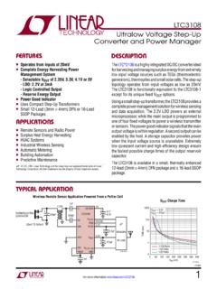
3 16-lead MSOP package with four pins removed. TYPICAL APPLICATION. 2 MHz, 48V Output Boost Converter Efficiency and Power Loss VOUT 100 H 48V. VIN 90 8V TO 38V 300mA AT VIN = 8V. F 640mA AT VIN = 12V 80 EFFICIENCY 1M 1A AT VIN = 24V. VIN SW 70 POWER LOSS (W). EFFICIENCY (%). LT8364 FBX F 60 EN/UVLO BIAS x2. 50 POWER LOSS. INTVCC 40 SYNC/MODE. RT SS GND VC 30 1 F 20 VIN = 12V. 20k 10 VIN = 24V. 10nF 0 0. 0 1 8364 TA01a LOAD CURRENT (A). 8364 TA01b Rev. A. Document Feedback For more information 1. LT8364 . ABSOLUTE MAXIMUM RATINGS. (Note 1). 60V 4V. VIN, 60V Operating Junction Temperature (Note 3). 40V LT8364E, 40 C to 125 C. EN/UVLO Pin Above VIN Pin, 6V 40 C to 150 C. INTVCC ..(Note 2) Storage Temperature 65 C to 150 C. VC .. 4V. PIN CONFIGURATION. TOP VIEW.
4 TOP VIEW. NC 1 12 SW1. EN/UVLO 1 16 SW1. EN/UVLO 2 11 SW2. VIN 3 17 14 SW2. PGND, VIN 3 13 10 SYNC/MODE. INTVCC 5 12 SYNC/MODE. GND GND. NC 6 11 SS INTVCC 4 9 SS. BIAS 7 10 RT. VC 8 9 FBX BIAS 5 8 RT. MSE PACKAGE VC 6 7 FBX. VARIATION: MSE16 (12). 16-LEAD PLASTIC MSOP DE PACKAGE. JA = 45 C/W, JC = 10 C/W 12-LEAD (4mm 3mm) PLASTIC DFN. EXPOSED PAD (PIN 17) IS PGND AND GND, MUST BE SOLDERED TO PCB JA = 43 C/W, JC = C/W. EXPOSED PAD (PIN 13) IS PGND AND GND, MUST BE SOLDERED TO PCB. ORDER INFORMATION. LEAD FREE FINISH TAPE AND REEL PART MARKING* PACKAGE DESCRIPTION TEMPERATURE RANGE. LT8364 EMSE#PBF LT8364 EMSE#TRPBF 8364 16-Lead Plastic MSOP with 4 Pins Removed 40 C to 125 C. LT8364 IMSE#PBF LT8364 IMSE#TRPBF 8364 16-Lead Plastic MSOP with 4 Pins Removed 40 C to 125 C.
5 LT8364 HMSE#PBF LT8364 HMSE#TRPBF 8364 16-Lead Plastic MSOP with 4 Pins Removed 40 C to 150 C. LT8364 EDE#PBF LT8364 EDE#TRPBF 8364 12-Lead (4mm 3mm) Plastic DFN 40 C to 125 C. LT8364 IDE#PBF LT8364 IDE#TRPBF 8364 12-Lead (4mm 3mm) Plastic DFN 40 C to 125 C. LT8364 HDE#PBF LT8364 HDE#TRPBF 8364 12-Lead (4mm 3mm) Plastic DFN 40 C to 150 C. AUTOMOTIVE PRODUCTS**. LT8364 EMSE#WPBF LT8364 EMSE#WTRPBF 8364 16-Lead Plastic MSOP with 4 Pins Removed 40 C to 125 C. LT8364 IMSE#WPBF LT8364 IMSE#WTRPBF 8364 16-Lead Plastic MSOP with 4 Pins Removed 40 C to 125 C. LT8364 HMSE#WPBF LT8364 HMSE#WTRPBF 8364 16-Lead Plastic MSOP with 4 Pins Removed 40 C to 150 C. Contact the factory for parts specified with wider operating temperature ranges. *The temperature grade is identified by a label on the shipping container.
6 Tape and reel specifications. Some packages are available in 500 unit reels through designated sales channels with #TRMPBF suffix. **Versions of this part are available with controlled manufacturing to support the quality and reliability requirements of automotive applications. These models are designated with a #W suffix. Only the automotive grade products shown are available for use in automotive applications. Contact your local Analog Devices account representative for specific product ordering information and to obtain the specific Automotive Reliability reports for these models. Rev. A. 2 For more information LT8364 . ELECTRICAL CHARACTERISTICS The l denotes the specifications which apply over the full operating temperature range, otherwise specifications are at TA = 25 C.
7 VIN = 12V, EN/UVLO = 12V unless otherwise noted. PARAMETER CONDITIONS MIN TYP MAX UNITS. VIN Operating Voltage Range l 60 V. VIN Quiescent Current at Shutdown VEN/UVLO = 1 2 A. l 1 15 A. VEN/UVLO = 2 5 A. l 2 25 A. VIN Quiescent Current Sleep Mode (Not Switching) SYNC = 0V 9 15 A. l 9 30 A. Active Mode (Not Switching) SYNC = 0V or INTVCC, BIAS = 0V 1200 1600 A. l 1200 1850 A. SYNC = 0V or INTVCC, BIAS = 5V 22 40 A. l 22 65 A. BIAS Threshold Rising, BIAS Can Supply INTVCC V. Falling, BIAS Cannot Supply INTVCC 4 V. VIN Falling Threshold to Supply INTVCC BIAS = 12V BIAS 2V V. BIAS Falling Threshold to Supply INTVCC VIN = 12V VIN V. FBX Regulation FBX Regulation Voltage FBX > 0V l V. FBX < 0V l V. FBX Line Regulation FBX > 0V, < VIN < 60V %/V. FBX < 0V, < VIN < 60V %/V.
8 FBX Pin Current FBX = , l 10 10 nA. Oscillator Switching Frequency (fOSC) RT = 165k l 265 300 327 kHz RT = l 1 MHz RT = 20k l 2 MHz SSFM Maximum Frequency Deviation f/fOSC 100, RT = 20k 14 20 28 %. Minimum On-Time Burst Mode, VIN = 24V (Note 6) 85 110 ns Pulse-Skip Mode, VIN = 24V (Note 6) 60 85 ns Minimum Off-Time l 50 75 ns SYNC/Mode, Mode Thresholds (Note 5) High (Rising) l V. Low (Falling) l V. SYNC/Mode, Clock Thresholds (Note 5) Rising l V. Falling l V. fSYNC/fOSC Allowed Ratio RT = 20k 1 kHz/kHz SYNC Pin Current SYNC = 2V 10 25 A. SYNC = 0V, Current Out of Pin 10 25 A. Switch Maximum Switch Current Limit Threshold l 4 5 A. Switch Overcurrent Threshold Discharges SS Pin A. Switch RDS(ON) ISW = 100 m . Switch Leakage Current VSW = 60V 1 A. Rev. A. For more information 3.
9 LT8364 . ELECTRICAL CHARACTERISTICS The l denotes the specifications which apply over the full operating temperature range, otherwise specifications are at TA = 25 C. VIN = 12V, EN/UVLO = 12V unless otherwise noted. PARAMETER CONDITIONS MIN TYP MAX UNITS. EN/UVLO Logic EN/UVLO Pin Threshold (Rising) Start Switching l V. EN/UVLO Pin Threshold (Falling) Stop Switching l V. EN/UVLO Pin Current VEN/UVLO = l 50 50 nA. Soft-Start Soft-Start Charge Current SS = 2 A. Soft-Start Pull-Down Resistance Fault Condition, SS = 220 . Error Amplifier Error Amplifier Transconductance FBX = 75 A/V. FBX = 60 A/V. Error Amplifier Voltage Gain FBX = 185 V/V. FBX = 145 V/V. Error Amplifier Max Source Current VC = , Current Out of Pin 7 A. Error Amplifier Max Sink Current VC = 7 A.
10 Note 1: Stresses beyond those listed under Absolute Maximum Ratings Note 4: The IC includes overtemperature protection that is intended to may cause permanent damage to the device. Exposure to any Absolute protect the device during overload conditions. Junction temperature will Maximum Rating condition for extended periods may affect device exceed 150 C when overtemperature protection is active. Continuous reliability and lifetime. operation above the specified maximum operating junction temperature Note 2: INTVCC cannot be externally driven. No additional components or will reduce lifetime. loading is allowed on this pin. Note 5: For SYNC/MODE inputs required to select modes of operation see Note 3: The LT8364E is guaranteed to meet performance specifications the Pin Functions and Applications Information sections.
