Transcription of LT8640/LT8640-1 42V, 5A Synchronous Step-Down Silent ...
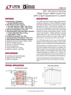
1 LT8640/LT8640-118640fbFor more information APPLICATION FEATURESDESCRIPTION42V, 5A Synchronous Step-Down Silent Switcher with A Quiescent CurrentThe LT 8640/LT8640-1 Step-Down regulator features Silent Switcher architecture designed to minimize EMI/EMC emis-sions while delivering high efficiency at frequencies up to 3 MHz. Assembled in a 3mm 4mm QFN, the monolithic construction with integrated power switches and inclusion of all necessary circuitry yields a solution with a minimal PCB footprint. An ultralow A quiescent current with the output in full regulation enables applications requiring highest efficiency at very small load currents. Transient response remains excellent and output voltage ripple is below 10mVP-P at any load, from zero to full current.
2 The LT86 40/LT86 40-1 allows high VIN to low VOUT conversion at high frequency with a fast minimum top switch on-time of 30ns. Operation is safe in overload even with a saturated features are included and easy to use: An open-drain PG pin signals when the output is in regulation. The SYNC/MODE pin selects between Burst Mode operation, spread spectrum mode, synchronization to an external clock, and either pulse-skipping (LT86 40) or forced continuous mode (LT86 40-1 ). Soft-start and tracking functionality is accessed via the TR/SS pin. An accurate enable threshold can be set using the EN/UV pin and a resistor at the RT pin programs switch 5A Step-Down ConverterAPPLICATIONS nSilent Switcher Architecture nUltralow EMI/EMC Emissions nSpread Spectrum Frequency Modulation nHigh Efficiency at High Frequency nUp to 96% Efficiency at 1 MHz, 12 VIN to 5 VOUT nUp to 95% Efficiency at 2 MHz, 12 VIN to 5 VOUT nWide Input Voltage Range: to 42V n5A Maximum Continuous Output, 7A Peak Transient Output nUltralow Quiescent Current Burst Mode Operation A IQ Regulating 12 VIN to nOutput Ripple < 10mVP-P nFast Minimum Switch On-Time: 30ns nLow Dropout Under All Conditions.
3 100mV at 1A nForced Continuous Mode (LT8640-1 Only) nSafely Tolerates Inductor Saturation in Overload nAdjustable and Synchronizable: 200kHz to 3 MHz nPeak Current Mode Operation nOutput Soft-Start and Tracking nSmall 18-Lead 3mm 4mm QFN nAutomotive and Industrial Supplies nGeneral Purpose Step-Down nGSM Power SuppliesAll registered trademarks and trademarks are the property of their respective owners. Protected by patents, including TA01aBSTSYNC/MODESWTR/SSBIASINTVCCFBRTGN D1 F1 MVOUT5V5A1 TO H243kGND2 GND1fSW = 1 MHzEFFICIENCYPOWER LOSS1 MHz, L = H2 MHz, L = H3 MHz, L = 1 HLOAD CURRENT (A) (%)POWER LOSS (W)12 VIN to 5 VOUT Ef ciency8640 TA01bLT8640/LT8640-128640fbFor more information CONFIGURATIONABSOLUTE MAXIMUM RATINGSVIN, EN/UV, PG.
4 42 VBIAS ..25 VFB, TR/SS ..4 VSYNC Voltage ..6 VOperating Junction Temperature Range (Note 2) LT86 40E/ LT86 40-1E .. 40 C to 125 C LT86 40I/ LT86 40-1I .. 40 C to 125 C LT86 40H/ LT86 40-1H .. 40 C to 150 CStorage Temperature Range .. 65 to 150 C(Note 1)ORDER INFORMATIONLEAD FREE FINISHTAPE AND REELPART MARKING*PACKAGE DESCRIPTIONTEMPERATURE RANGELT8640 EUDC#PBFLT8640 EUDC#TRPBFLGNJ18-Lead (3mm 4mm) Plastic QFN 40 C to 125 CLT8640 IUDC#PBFLT8640 IUDC#TRPBFLGNJ18-Lead (3mm 4mm) Plastic QFN 40 C to 125 CLT8640 HUDC#PBFLT8640 HUDC#TRPBFLGNJ18-Lead (3mm 4mm) Plastic QFN 40 C to 150 CLT8640 EUDC-1#PBFLT8640 EUDC-1#TRPBFLGVT18-Lead (3mm 4mm) Plastic QFN 40 C to 125 CLT8640 IUDC-1#PBFLT8640 IUDC-1#TRPBFLGVT18-Lead (3mm 4mm) Plastic QFN 40 C to 125 CLT8640 HUDC-1#PBFLT8640 HUDC-1#TRPBFLGVT18-Lead (3mm 4mm) Plastic QFN 40 C to 150 CConsult LTC Marketing for parts specified with wider operating temperature ranges.
5 *The temperature grade is identified by a label on the shipping more information on lead free part marking, go to: For more information on tape and reel specifications, go to: Some packages are available in 500 unit reels through designated sales channels with #TRMPBF VIEWUDC PACKAGE18-LEAD (3mm 4mm) PLASTIC QFN1 BIASINTVCCBSTVIN1 GND1TR/SSRTEN/UVVIN2 GND2 GND1 SWSWGND2 FBPGGNDSYNC/MODE1615141311234621SW22SW JA = 40 C/W, JC(PAD) = 12 C/W (Note 3) EXPOSED PAD (PINS 21, 22) ARE SW, SHOULD BE SOLDERED TO PCBNOTE: PINS 5 AND 12 ARE REMOVED. CONFIGURATION DOES NOT MATCH JEDEC 20-LEAD PACKAGE #orderinfoLT8640/LT8640-138640fbFor more information CHARACTERISTICS The l denotes the specifications which apply over the full operating temperature range, otherwise specifications are at TA = 25 Input Quiescent CurrentVEN/UV = 0V 10 A AVEN/UV = 2V, Not Switching, VSYNC = 0V 10 A AVEN/UV = 2V, Not Switching, VSYNC = 2V (LT8640 Only)
6 Current in RegulationVOUT = , VIN = 6V, Output Load = 100 A VOUT = , VIN = 6V, Output Load = 1mAl l21 22050 350 A AFeedback Reference VoltageVIN = 6V, ILOAD = VIN = 6V, ILOAD = VFeedback Voltage Line RegulationVIN = to Pin Input CurrentVFB = 1V 2020nABIAS Pin Current ConsumptionVBIAS = , ILOAD = 1A, 2 MHz11mAMinimum On-TimeILOAD = , SYNC = 0V ILOAD = , SYNC = l35 3050 50ns nsMinimum Off-Time80110nsOscillator FrequencyRT = 221k, ILOAD = 1A RT = , ILOAD = 1A RT = , ILOAD = 1Al l l180 665 700 735 kHz MHzTop Power NMOS On-ResistanceISW = 1A67m Top Power NMOS Current Power NMOS On-ResistanceVINTVCC = , ISW = 1A28m SW Leakage CurrentVIN = 42V, VSW = 0V, 42V 1515 AEN/UV Pin ThresholdEN/UV Pin Hysteresis 40mVEN/UV Pin CurrentVEN/UV = 2V 2020nAPG Upper Threshold Offset from VFBVFB Lower Threshold Offset from VFBVFB Risingl 8 LeakageVPG = 4040nAPG Pull-Down ResistanceVPG = SYNC/MODE ThresholdSYNC/MODE DC and Clock Low Level Voltage SYNC/MODE Clock High Level Voltage SYNC/MODE DC High Level V VSpread Spectrum Modulation Frequency RangeRT = , VSYNC = Spectrum Modulation FrequencyVSYNC = Source ATR/SS Pull-Down ResistanceFault Condition, TR/SS = LT8640/LT8640-148640fbFor more information CHARACTERISTICSNote 1: Stresses beyond those listed under Absolute Maximum Ratings may cause permanent damage to the device.
7 Exposure to any Absolute Maximum Rating condition for extended periods may affect device reliability and 2: The LT8640E/LT8640-1E is guaranteed to meet performance specifications from 0 C to 125 C junction temperature. Specifications over the 40 C to 125 C operating junction temperature range are assured by design, characterization, and correlation with statistical process controls. The LT8640I/LT8640-1I is guaranteed over the full 40 C to 125 C operating junction temperature range. The LT8640H/LT8640-1H is guaranteed over the full 40 C to 150 C operating junction temperature range. High junction temperatures degrade operating lifetimes. Operating lifetime is derated at junction temperatures greater than 125 C. The junction temperature (TJ, in C) is calculated from the ambient The l denotes the specifications which apply over the full operating temperature range, otherwise specifications are at TA = 25 Output Sink Current in Forced Continuous ModeVFB = , L = H, RT = VIN to Disable Forced Continuous ModeVIN Rising353739 VLT8640-1 VFB Offset from Feedback Reference Voltage to Disable Forced Continuous ModeVFB (TA in C) and power dissipation (PD, in Watts) according to the formula: TJ = TA + (PD JA)where JA (in C/W) is the package thermal 3: values determined per JEDEC 51-7, 51-12.
8 See Applications Information section for information on improving the thermal resistance and for actual temperature measurements of a demo board in typical operating 4: This IC includes overtemperature protection that is intended to protect the device during overload conditions. Junction temperature will exceed 150 C when overtemperature protection is active. Continuous operation above the specified maximum operating junction temperature will reduce more information PERFORMANCE CHARACTERISTICSE fficiency at vs FrequencyBurst Mode Operation Efficiency vs Inductor ValueReference Voltage12 VIN to Efficiency vs FrequencyEfficiency at 5 VOUTLOAD CURRENT (A) (%)POWER LOSS (W) , L = H2 MHz, L = 1 H3 MHz, L = 1 H L = WE LHMI1040 EFFICIENCYPOWER LOSSE fficiency at 5 VOUTE fficiency at G03 LOAD CURRENT (A) (%)POWER LOSS (W) = 12 VVIN = 24 VVIN = 36 VfSW = 1 MHzL = IHLP3232DZ-01, HEFFICIENCYPOWER LOSS8640 G04 LOAD CURRENT (A) (%)POWER LOSS (W) = 12 VVIN = 24 VVIN = 36 VfSW = 1 MHzL = IHLP3232DZ-01, HEFFICIENCYPOWER LOSSLOAD CURRENT (mA)40 EFFICIENCY (%)
9 506070808640 1 10 100 1000 VIN = 12 VVIN = 24 VVIN = 36 VfSW = 1 MHzL = IHLP3232DZ-01, HLOAD CURRENT (mA)40 EFFICIENCY (%)506070808640 1 10 100 1000 VIN = 12 VVIN = 24 VVIN = 36 VfSW = 1 MHzL = IHLP3232DZ-01, HSWITCHING FREQUENCY (MHz) (%)VIN = 12 VVOUT = = 2AL = IHLP3232DZ-01, HINDUCTOR VALUE ( H)165 EFFICIENCY (%)7075808590952345678640 G088 VIN = 12 VVIN = 24 VVOUT = 5 VILOAD = 10mAL = IHLP3232DZ-01 TEMPERATURE ( C) 50 REFERENCE VOLAGE (V) LOSSL = WE LHMI10401 MHz, L = H2 MHz, L = H3 MHz, L = 1 HLOAD CURRENT (A) (%)POWER LOSS (W)vs Frequency12 VIN to 5 VOUT Ef ciency8640 G01LT8640/LT8640-168640fbFor more information PERFORMANCE CHARACTERISTICSTop FET Current Limit vs Duty CycleTop FET Current LimitSwitch DropEN Pin ThresholdsLoad RegulationLine RegulationTEMPERATURE ( C) 50EN THRESHOLD (V) RISINGEN FALLINGLOAD CURRENT (A)0 IN VOUT (%) = 5 VVIN = 12VR1/R2 = 100 VOLTAGE (V)5 IN VOUT (%) = 5 VILOAD = 1AR1/R2 = 100 LIMIT (A)8640 G14 TEMPERATURE ( C) LIMIT (A) 25751258640 DCTEMPERATURE ( C) 50 SWITCH DROP (mV)1001508640 G16500050100 2525751251507512525 SWITCH CURRENT = 1 ABOTTOM SWITCHTOP SWITCHSWITCH CURRENT (A)00 SWITCH DROP (mV)
10 50150200250500350128640 G17100400450300354 TOP SWITCHBOTTOM SWITCHILOAD = 2 AVSYNC = FLOATVSYNC = 0 VTEMPERATURE ( C) 50 25025507510012525283134374043 MINIMUM ON-TIME (ns)8640 G18 Minimum On-TimeSwitch DropVOUT = = HIN REGULATIONINPUT VOLTAGE (V) CURRENT ( A)No-Load Supply Current8640 G13LT8640/LT8640-178640fbFor more information PERFORMANCE CHARACTERISTICSD ropout VoltageSwitching FrequencyBurst FrequencyFrequency FoldbackMinimum Load to Full Frequency (Pulse-Skipping Mode)Soft-Start TrackingSoft-Start CurrentPG High ThresholdsPG Low ThresholdsLOAD CURRENT (A)0 DROPOUT VOLTAGE (mV) = 5 VVOUT SET TO REGULATE AT 5VL = IHLP3232DZ-01, 1 HTEMPERATURE ( C) 50 SWITCHING FREQUENCY (kHz)730258640 G20700680 25050670660740RT = VOLTAGE (V)0 SWITCHING FREQUENCY (kHz) = = 12 VVSYNC = 0 VRT = VOLTAGE (V)0FB VOLTAGE (V) ( C) 50SS PIN CURRENT ( A) = ( C) THRESHOLD OFFSET FROM VREF (%) 2525150125FB FALLINGFB RISINGTEMPERATURE ( C) 50 THRESHOLD OFFSET FROM VREF (%) 1258640 G27 2525150FB FALLINGFB RISINGLOAD CURRENT (mA)00 SWITCHING FREQUENCY (kHz)20040060080010001200100200300400864 0 G21 FRONT PAGE APPLICATIONVIN = 12 VVOUT = 5 VINPUT VOLTAGE (V)5 LOAD CURRENT (mA)60801002030458640 G22402001015253540 FRONT PAGE APPLICATIONVOUT =