Transcription of LTC2323-12 - Dual, 12-Bit + Sign, 5Msps Differential Input ...
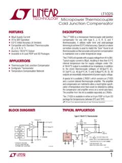
1 LTC2323-12 . Dual, 12-Bit + Sign, 5 Msps Differential Input ADC with Wide Input Common Mode Range FEATURES DESCRIPTION. nn 5 Msps Throughput Rate The LTC 2323-12 is a low noise, high speed dual nn INL (Typ) 12-Bit + sign successive approximation register (SAR). nn Guaranteed 12-Bit , No Missing Codes ADC with Differential inputs and wide Input common mode nn 8V. P-P Differential Inputs with Wide Input Common range. Operating from a single or 5V supply, the Mode Range LTC2323-12 has an 8VP-P Differential Input range, making nn 73dB SNR (Typ) at f = 2 MHz it ideal for applications which require a wide dynamic IN. nn 85dB THD (Typ) at f = 2 MHz range with high common mode rejection. The LTC2323- IN. nn Guaranteed Operation to 125 C 12 achieves INL typical, no missing codes at 12. nn Single or 5V Supply bits and 73dB SNR. nn Low Drift (20ppm/ C Max) or Internal The LTC2323-12 has an onboard low drift (20ppm/ C max). Reference or temperature-compensated reference. nn to I/O Voltages The LTC2323-12 also has a high speed SPI-compatible nn CMOS or LVDS SPI-Compatible Serial I/O.
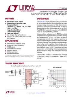
2 Serial interface that supports CMOS or LVDS. The fast nn Power Dissipation 38mW/Ch (Typ). 5 Msps per channel throughput with one-cycle latency nn Small 28-Lead (4mm 5mm) QFN Package makes the LTC2323-12 ideally suited for a wide variety of high speed applications. The LTC2323-12 dissipates only APPLICATIONS 38mW per channel and offers nap and sleep modes to nn High Speed Data Acquisition Systems reduce the power consumption to 5 W for further power nn Communications savings during inactive periods. nn Remote Data Acquisition L, LT, LTC, LTM, Linear Technology and the Linear logo are registered trademarks of Analog nn Imaging Devices, Inc. All other trademarks are the property of their respective owners. nn Optical Networking nn Automotive nn Multiphase Motor Control TYPICAL APPLICATION. 16k Point FFT fS = 5 Msps, fIN = Differential INPUTS OR 5V. NO CONFIGURATION REQUIRED. 0. 10 F. SNR = 73dBFS. IN+, IN . THD = 86dB. 20 SINAD = INSTRUMENTATION Differential VDD REFOUT1. 25.
3 SFDR = 88dB. 10 F. AIN1+. AMPLITUDE (dBFS). VBYP1 40. 1 F. LTC2323-12 . 0V 0V REFOUT2. 220pF. 10 F 60. VBYP2. BIPOLAR UNIPOLAR 1 F. 80. 25 . AIN1 SDO1 TO CONTROL. AIN2+ SDO2 LOGIC 100. AIN2 CLKOUT (FPGA, CPLD, 0V 0V. VDD CMOS/LVDS SCK DSP, ETC.). REFINT CNV. 120. GND OGND OVDD TO 0 1 2 1 F. 232312 TA01a FREQUENCY (MHz) 232312 TA01b 232312fb For more information 1. LTC2323-12 . ABSOLUTE MAXIMUM RATINGS PIN CONFIGURATION. (Notes 1, 2). Supply Voltage (VDD)..6V TOP VIEW. Supply Voltage (OVDD)..3V. CMOS/LVDS. REFRTN2. REFOUT2. Supply Bypass Voltage (VBYP1, VBYP2)..3V. REFINT. VBYP2. OGND. Analog Input Voltage 28 27 26 25 24 23. AIN+, AIN (Note 3).. to (VDD + ) VDD 1 22 SCK . REFOUT1, . to (VDD + ) AIN2+ 2 21 SCK+. CNV (Note 15).. to (VDD + ) AIN2 3 20 SDO2 . Digital Input Voltage GND 4 29 19 SDO2+. GND. (Note 3).. (GND ) to (OVDD + ) GND 5 18 CLKOUT . Digital Output Voltage AIN1 6 17 CLKOUT+. AIN1+ 7 16 SDO1 . (Note 3).. (GND ) to (OVDD + ). VDD 8 15 SDO1+. Power 9 10 11 12 13 14.
4 Operating Temperature Range CNV. GND. REFRTN1. REFOUT1. VBYP1. OVDD. 0 C to 70 C. 40 C to 85 C. UFD PACKAGE. 40 C to 125 C 28-LEAD (4mm 5mm) PLASTIC QFN. Storage Temperature 65 C to 150 C TJMAX = 125 C, JA = 43 C/W. EXPOSED PAD (PIN 29) IS GND, MUST BE SOLDERED TO PCB. ORDER INFORMATION #orderinfo LEAD FREE FINISH TAPE AND REEL PART MARKING* PACKAGE DESCRIPTION TEMPERATURE RANGE. LTC2323 CUFD-12#PBF LTC2323 CUFD-12#TRPBF 23232 28-Lead (4mm 5mm) Plastic QFN 0 C to 70 C. LTC2323 IUFD-12#PBF LTC2323 IUFD-12#TRPBF 23232 28-Lead (4mm 5mm) Plastic QFN 40 C to 85 C. LTC2323 HUFD-12#PBF LTC2323 HUFD-12#TRPBF 23232 28-Lead (4mm 5mm) Plastic QFN 40 C to 125 C. Consult LTC Marketing for parts specified with wider operating temperature ranges. *The temperature grade is identified by a label on the shipping container. For more information on lead free part marking, go to: For more information on tape and reel specifications, go to: Some packages are available in 500 unit reels through designated sales channels with #TRMPBF suffix.
5 ELECTRICAL CHARACTERISTICS. The l denotes the specifications which apply over the full operating temperature range, otherwise specifications are at TA = 25 C (Note 4). SYMBOL PARAMETER CONDITIONS MIN TYP MAX UNITS. VIN+ Absolute Input Range (AIN1+, AIN2+) (Note 5) l 0 VDD V. VIN Absolute Input Range (AIN1 , AIN2 ) (Note 5) l 0 VDD V. VIN+ VIN Input Differential Voltage Range VIN = VIN+ VIN l REFOUT1,2 REFOUT1,2 V. VCM Common Mode Input Range VIN = (VIN+ + VIN )/2 l 0 VDD V. IIN Analog Input DC Leakage Current l 1 1 A. CIN Analog Input Capacitance 10 pF. CMRR Input Common Mode Rejection Ratio fIN = 85 dB. IREFOUT External Reference Current REFINT = 0V, REFOUT = 675 A. 232312fb 2 For more information LTC2323-12 . CONVERTER CHARACTERISTICS. The l denotes the specifications which apply over the full operating temperature range, otherwise specifications are at TA = 25 C (Notes 4, 16). SYMBOL PARAMETER CONDITIONS MIN TYP MAX UNITS. Resolution l 12 Bits No Missing Codes l 12 Bits Transition Noise LSBRMS.
6 INL Integral Linearity Error (Note 6) l 1 1 LSB. DNL Differential Linearity Error l LSB. BZE Bipolar Zero-Scale Error (Note 7) l 3 0 3 LSB. Bipolar Zero-Scale Error Drift LSB/ C. FSE Bipolar Full-Scale Error VREFOUT1,2 = (REFINT Grounded) (Note 7) l 20 3 20 LSB. Bipolar Full-Scale Error Drift VREFOUT1,2 = (REFINT Grounded) 15 ppm/ C. DYNAMIC ACCURACY. The l denotes the specifications which apply over the full operating temperature range, otherwise specifications are at TA = 25 C and AIN = 1dBFS (Notes 4, 8). SYMBOL PARAMETER CONDITIONS MIN TYP MAX UNITS. SINAD Signal-to-(Noise + Distortion) Ratio fIN = , VREFOUT1,2 = , Internal Reference l dB. fIN = , VREFOUT1,2 = 5V, External Reference dB. SNR Signal-to-Noise Ratio fIN = , VREFOUT1,2 = , Internal Reference l 70 73 dB. fIN = , VREFOUT1,2 = 5V, External Reference dB. THD Total Harmonic Distortion fIN = , VREFOUT1,2 = , Internal Reference l 85 80 dB. fIN = , VREFOUT1,2 = 5V, External Reference 84 dB. SFDR Spurious Free Dynamic Range fIN = , VREFOUT1,2 = , Internal Reference l 78 88 dB.
7 FIN = , VREFOUT1,2 = 5V, External Reference 88 dB. 3dB Input Linear Bandwidth 10 MHz Aperture Delay 500 ps Aperture Delay Matching 500 ps Aperture Jitter 1 psRMS. Transient Response Full-Scale Step 3 ns INTERNAL REFERENCE CHARACTERISTICS. The l denotes the specifications which apply over the full operating temperature range, otherwise specifications are at TA = 25 C (Note 4). SYMBOL PARAMETER CONDITIONS MIN TYP MAX UNITS. VREFOUT1,2 Internal Reference Output Voltage < VDD < l V. < VDD < l VREFOUT1,2 Temperature Coefficient (Note 14) l 3 20 ppm/ C. REFOUT1,2 Output Impedance . VREFOUT1,2 Line Regulation VDD = to mV/V. 232312fb For more information 3. LTC2323-12 . DIGITAL INPUTS AND DIGITAL OUTPUTS. The l denotes the specifications which apply over the full operating temperature range, otherwise specifications are at TA = 25 C (Note 4). SYMBOL PARAMETER CONDITIONS MIN TYP MAX UNITS. VIH High Level Input Voltage l OVDD V. VIL Low Level Input Voltage l OVDD V. IIN Digital Input Current VIN = 0V to OVDD l 10 10 A.
8 CIN Digital Input Capacitance 5 pF. VOH High Level Output Voltage IO = -500 A l OVDD V. VOL Low Level Output Voltage IO = 500 A l V. IOZ Hi-Z Output Leakage Current VOUT = 0V to OVDD l 10 10 A. ISOURCE Output Source Current VOUT = 0V 10 mA. ISINK Output Sink Current VOUT = OVDD 10 mA. VID LVDS Differential Input Voltage 100 Differential Termination, OVDD = l 240 600 mV. VIS LVDS Common Mode Input Voltage 100 Differential Termination, OVDD = l 1 V. VOD LVDS Differential Output Voltage 100 Differential Load, LVDS Mode, l 100 150 300 mV. OVDD = VOS LVDS Common Mode Output Voltage 100 Differential Load, LVDS Mode, l V. OVDD = VOD_LP Low Power LVDS Differential Output 100 Differential Load, Low Power, l 75 100 200 mV. Voltage LVDS Mode ,OVDD = VOS_LP Low Power LVDS Common Mode 100 Differential Load, Low Power, l V. Output Voltage LVDS Mode ,OVDD = POWER REQUIREMENTS. The l denotes the specifications which apply over the full operating temperature range, otherwise specifications are at TA = 25 C (Note 4).
9 SYMBOL PARAMETER CONDITIONS MIN TYP MAX UNITS. VDD Supply Voltage 5V Operation l V. Operation l V. OVDD Supply Voltage l V. IVDD Supply Current 5 Msps Sample Rate (IN+ = IN = 0V) l 14 18 mA. IOVDD Supply Current 5 Msps Sample Rate (CL = 5pF) CMOS Mode l 5 mA. 5 Msps Sample Rate (RL = 100 ) LVDS Mode l 12 mA. INAP Nap Mode Current Conversion Done (IVDD) l 5 mA. ISLEEP Sleep Mode Current Sleep Mode (IVDD + IOVDD) CMOS Mode l 1 5 A. Sleep Mode (IVDD + IOVDD) LVDS Mode l 1 5 A. Power Dissipation VDD = 5 Msps Sample Rate (IN+ = IN = 0V) CMOS Mode l 55 58 mW. VDD = 5 Msps Sample Rate (IN+ = IN = 0V) LVDS Mode l 72 86 mW. Nap Mode VDD = Conversion Done (IVDD + IOVDD) CMOS Mode l 9 13 mW. VDD = Conversion Done (IVDD + IOVDD) LVDS Mode l 32 41 mW. Sleep Mode VDD = Sleep Mode (IVDD + IOVDD) CMOS Mode l 5 W. VDD = Sleep Mode (IVDD + IOVDD) LVDS Mode l 5 W. PD_5V Power Dissipation VDD = 5V 5 Msps Sample Rate (IN+ = IN = 0V) CMOS Mode l 76 100 mW. VDD = 5V 5 Msps Sample Rate (IN+ = IN = 0V) LVDS Mode l 105 110 mW.
10 Nap Mode VDD = 5V Conversion Done (IVDD + IOVDD) CMOS Mode l 15 25 mW. VDD = 5V Conversion Done (IVDD + IOVDD) LVDS Mode l 38 40 mW. Sleep Mode VDD = 5V Sleep Mode (IVDD + IOVDD) CMOS Mode l 5 25 W. VDD = 5V Sleep Mode (IVDD + IOVDD) LVDS Mode l 5 25 W. 232312fb 4 For more information LTC2323-12 . ADC TIMING CHARACTERISTICS. The l denotes the specifications which apply over the full operating temperature range, otherwise specifications are at TA = 25 C (Note 4). SYMBOL PARAMETER CONDITIONS MIN TYP MAX UNITS. fSMPL Maximum Sampling Frequency l 5 Msps tCYC Time Between Conversions (Note 11) l 200 1000000 ns tCONV Conversion Time l ns tCNVH CNV High Time l 35 ns tDCNVSCKL SCK Quiet Time from CNV (Note 11) l 10 ns tDSCKLCNVH SCK Delay Time to CNV (Note 11) l 20 ns tSCK SCK Period (Notes 12, 13) l ns tSCKH SCK High Time l 4 ns tSCKL SCK Low Time l 4 ns tDSCKCLKOUT SCK to CLKOUT Delay (Note 12) l ns tDCLKOUTSDOV SDO Data Valid Delay from CLKOUT CL = 5pF (Note 12) l 2 ns tHSDO SDO Data Remains Valid Delay from CL = 5pF (Note 11) l 2 ns CLKOUT.
