Transcription of LTC3864 - 60V Low IQ Step-Down DC/DC Controller …
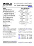
1 LTC386413864faFor more information applicaTion FeaTuresDescripTion60V Low IQ Step-Down DC/DC Controller with 100% Duty Cycle CapabilityThe LT C 3864 is a robust, high voltage Step-Down DC/DC Controller optimized for automotive and industrial applica-tions. It drives a P-channel power MOSFET switch allowing 100% duty cycle operation. The wide input and output volt-age ranges cover a multitude of applications. This device has been verified with the failure mode and effects analysis (FMEA) procedure for operation during failure conditions. The LTC3864 offers excellent light load efficiency, draw-ing only 40 A quiescent current in a user programmable Burst Mode operation. Its peak current mode, constant frequency PWM architecture provides for good control of switching frequency and output current limit.
2 The switch-ing frequency can be programmed from 50kHz to 850kHz with an external resistor and can be synchronized to an external clock from 75kHz to 750kHz. The LTC3864 offers programmable soft-start or output tracking. Safety features include overvoltage protection, overcurrent and short-circuit protection including fre-quency foldback and a power good output signal. The LTC3864 is available in thermally enhanced 12-Pin MSOP and 3mm 4mm DFN to 60V Input, 5V/2A Output, 350kHz Step-Down ConverterapplicaTionsn Wide Operating VIN Range: to 60Vn Wide VOUT Range: to VINn Low Operating IQ = 40 An Very Low Dropout Operation: 100% Duty Cyclen Strong High Voltage MOSFET Gate Drivern Constant Frequency Current Mode Architecturen Verified FMEA for Adjacent Pin Open/Shortn Selectable High Efficiency Burst Mode Operation or Pulse-Skipping Mode at Light Loadsn Programmable Fixed Frequency: 50kHz to 850kHzn Phase-Lockable Frequency.
3 75kHz to 750kHzn Accurate Current Limitn Programmable Soft-Start or Voltage Trackingn Internal Soft-Start Guarantees Smooth Start-Upn Power Good Output Voltage Monitorn Low Shutdown IQ = 7 An Available in Small 12-Pin Thermally Enhanced MSOP and DFN Packagesn Industrial and Automotive Power Suppliesn Telecom Power Suppliesn Distributed Power SystemsL, LT, LTC, LTM, OPTI-LOOP, Linear Technology, Burst Mode and the Linear logo are registered trademarks and Hot Swap is a trademark of Linear Technology Corporation. All other trademarks are the property of their respective owners. Protected by Patents including 10 F10 FPGNDLTC38643864 TA01 F 2 VOUT* * TO *VOUT FOLLOWS VIN WHEN VIN CURRENT (A) (%) TA01bPULSE-SKIPPINGB urst ModeOPERATIONVIN = 12 VVOUT = 5 VLTC386423864faFor more information conFiguraTionabsoluTe MaxiMuM raTingsInput Supply Voltage (VIN).
4 To 65 VVIN-VSENSE Voltage .. to 6 VVIN-VCAP Voltage .. to 10 VRUN to 65 VPGOOD, PLLIN/MODE Voltages .. to 6 VSS, ITH, FREQ, VFB Voltages .. to 5V(Note 1)12111098713 PGND123456 GATEVINSENSECAPRUNPGOODPLLIN/MODEFREQSGN DSSVFBITHTOP VIEWDE PACKAGE12-LEAD (4mm 3mm) PLASTIC DFN TJMAX = 150 C, JA = 43 C/W, JC = C/W EXPOSED PAD (PIN 13) IS PGND, MUST BE SOLDERED TO PCB FOR OPTIMAL THERMAL PERFORMANCE123456 PLLIN/MODEFREQSGNDSSVFBITH121110987 GATEVINSENSECAPRUNPGOODTOP VIEW13 PGNDMSE PACKAGE12-LEAD PLASTIC MSOP TJMAX = 150 C, JA = 40 C/W, JC = 10 C/WEXPOSED PAD (PIN 13) IS PGND, MUST BE SOLDERED TO PCB FOR OPTIMAL THERMAL PERFORMANCEorDer inForMaTionLEAD FREE FINISHTAPE AND REELPART MARKING*PACKAGE DESCRIPTIONTEMPERATURE RANGELTC3864 EMSE#PBFLTC3864 EMSE#TRPBF386412-Lead Plastic MSOP 40 C to 125 CLTC3864 IMSE#PBFLTC3864 IMSE#TRPBF386412-Lead Plastic MSOP 40 C to 125 CLTC3864 HMSE#PBFLTC3864 HMSE#TRPBF386412-Lead Plastic MSOP 40 C to 150 CLTC3864 MPMSE#PBFLTC3864 MPMSE#TRPBF386412-Lead Plastic MSOP 55 C to 150 CLTC3864 EDE#PBFLTC3864 EDE#TRPBF386412-Lead (4mm 3mm) Plastic DFN 40 C to 125 CLTC3864 IDE#PBFLTC3864 IDE#TRPBF386412-Lead (4mm 3mm) Plastic DFN 40 C to 125 CLTC3864 HDE#PBFLTC3864 HDE#TRPBF386412-Lead (4mm 3mm) Plastic DFN 40 C to 150 CLTC3864 MPDE#PBFLTC3864 MPDE#TRPBF386412-Lead (4mm 3mm)
5 Plastic DFN 55 C to 150 CConsult LTC Marketing for parts specified with wider operating temperature ranges. *The temperature grade is identified by a label on the shipping LTC Marketing for information on non-standard lead based finish more information on lead free part marking, go to: For more information on tape and reel specifications, go to: Junction Temperature Range (Notes 2, 3, 4) LTC3864E,I .. 40 C to 125 C LTC386 4H .. 40 C to 150 C LTC386 4MP .. 55 C to 150 CStorage Temperature Range .. 65 C to 150 CLead Temperature (Soldering, 10 sec) MSOP Package ..300 C LTC386433864faFor more information characTerisTicsSYMBOLPARAMETERCONDITIONS MINTYPMAXUNITSI nput SupplyVINI nput Voltage Operating Lockout(VIN-VCAP) Ramping Up Threshold (VIN-VCAP) Ramping Down Threshold Hysteresisl l V V VIQI nput DC Supply CurrentPulse-Skipping ModePLLIN/MODE = 0V, FREQ = 0V, VFB = (No Load) mABurst Mode OperationPLLIN/MODE = Open, FREQ = 0V, VFB = (No Load)4060 AShutdown Supply CurrentRUN = 0V712 AOutput SensingVREGR egulated Feedback VoltageVITH = (Note 5) VREG VINF eedback Voltage Line RegulationVIN = to 60V (Note 5) VREG VITHF eedback Voltage Load RegulationVITH = to (Note 5) (EA)Error Amplifier TransconductanceVITH = , IITH = 5 A (Note 5) Input Bias Current 50 1050nACurrent SensingVILIMC urrent Limit Threshold (VIN-VSENSE)
6 VFB = Pin Input CurrentVSENSE = AStart-Up and ShutdownVRUNRUN Pin Enable ThresholdVRUN Pin Hysteresis150mVISSSoft-Start Pin Charging CurrentVSS = 0V10 ASwitching Frequency and Clock SynchronizationfProgrammable Switching FrequencyRFREQ = RFREQ = RFREQ = 105k 375105 440 810 505kHz kHz kHzfLOLow Switching FrequencyFREQ = 0V320350380kHzfHIHigh Switching FrequencyFREQ = Open485535585kHzfSYNCS ynchronization Frequencyl75750kHzVCLK(IH)Clock Input High Level into PLLIN/MODEl2 VVCLK(LO)Clock Input Low Level into Frequency as Percentage of Programmable FrequencyVFB = 0V, FREQ = 0V18%tON(MIN)Minimum On-Time220nsGate DriverVCAPGate Bias LDO Output Voltage (VIN-VCAP)IGATE = Bias LDO Dropout VoltageVIN = 5V, IGATE = VCAP(LINE)Gate Bias LDO Line Regulation9V VIN 60V, IGATE = VCAP(LOAD)Gate Bias LDO Load RegulationLoad = 0mA to 20mA The l denotes the specifications which apply over the specified operating junction temperature range, otherwise specifications are at TA = 25 C.
7 (Notes 3, 4) VIN = 12V, unless otherwise more information Pull-Up ResistanceGate High2 RDNGate Pull-Down ResistanceGate PGOOD and OvervoltageVPGLPGOOD Voltage LowIPGOOD = Leakage CurrentVPGOOD = 5V1 A%PGDPGOOD Trip LevelVFB Ramping Negative with Respect to VREG Hysteresis 13 10 7% %VFB Ramping Positive with Respect to VREG Hysteresis710 %tPGDLYPGOOD DelayPGOOD Going High to Low PGOOD Going Low to High100 100 s sVFBOVVFB Overvoltage Lockout ThresholdGATE Going High without Delay, VFB(OV)-VFB(NOM) in Percent10%elecTrical characTerisTics The l denotes the specifications which apply over the specified operating junction temperature range, otherwise specifications are at TA = 25 C.
8 (Notes 3, 4) VIN = 12V, unless otherwise 1: Stresses beyond those listed under Absolute Maximum Ratings may cause permanent damage to the device. Exposure to any Absolute Maximum Rating condition for extended periods may affect device reliability and 2: Continuous operation above the specified maximum operating junction temperature may impair device reliability or permanently damage the device. Note 3: The junction temperature (TJ in C) is calculated from the ambient temperature (TA in C) and power dissipation (PD in Watts) as follows: TJ = TA + (PD JA)where JA (in C/W) is the package thermal impedance provided in the Pin Configuration section for the corresponding 4: The LTC3864 is tested under pulsed loading conditions such that TJ TA. The LTC3864E is guaranteed to meet performance specifications from 0 C to 85 C operating junction temperature range.
9 The LTC3864E specifications over the 40 C to 125 C operating junction temperature range are assured by design, characterization and correlation with statistical process controls. The LTC3864I is guaranteed to meet performance specifications over the 40 C to 125 C operating junction temperature range, the LTC3864H is guaranteed over the 40 C to 150 C operating junction temperature range, and the LTC3864MP is guaranteed and tested over the full 55 C to 150 C operating junction temperature range. High junction temperatures degrade operating lifetimes; operating lifetime is derated for junction temperatures greater than 125 C. The maximum ambient temperature consistent with these specifications is determined by specific operating conditions in conjunction with board layout, the rated package thermal impedance and other environmental factors.
10 Note 5: The LTC3864 is tested in a feedback loop that adjust VFB to achieve a specified error amplifier output voltage (on ITH pin). LTC386453864faFor more information perForMance characTerisTicsTransient Response: Burst Mode OperationDropout Behavior (100% Duty Cycle)Low VIN OperationNormal Soft Start-UpSoft Start-Up into a Prebiased OutputOutput TrackingPulse-Skipping Mode Operation WaveformsBurst Mode Operation WaveformsTransient Response: Pulse-Skipping Mode OperationTA = 25 C, unless otherwise = 12V, VOUT = 5V FIGURE 8 CIRCUITVOUT1V/DIVSS200mV/DIVVIN5V/DIV1ms /DIV3864 G07 VIN = 12V, VOUT = 5 VILOAD = FIGURE 8 CIRCUITSS200mV/DIVVOUT1V/DIVRUN5V/DIV1ms /DIV3864 G08 VOUT PREBIASEDTO = 12V, VOUT = 5 VILOAD = 100mA FIGURE 8 CIRCUITVOUT2V/DIVSS200mV/DIV20ms/DIV3864 G09 VIN TRANSIENT: 12V TO 4V AND BACK TO 12 VVOUT = 5V, ILOAD = 100mA, FIGURE 8 CIRCUITGATE10V/DIVVOUT2V/DIVVIN2V/DIV50m s/DIV3864 G05 VOUT = VIN IN DROPOUTVIN = 0V TO THEN BACK TO 0 VILOAD = 100mAFIGURE 8 CIRCUITSW5V/DIVVOUT1V/DIVVIN1V/DIV20ms/D IV3864 G06 VOUT PROGRAMMED TO 5V.