Transcription of LTC6101 (Rev I) - Analog Devices
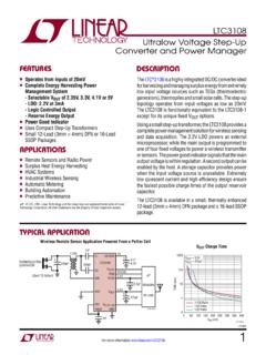
1 LTC6101 /LTC6101HV1 Rev IFor more information FeedbackTYPICAL APPLICATIONFEATURESAPPLICATIONSDESCRIPTI ONHigh Voltage,High-Side Current SenseAmplifier in SOT-23TO P6101 VOUTV+V OUT IN+INVSENSEILOAD5V TO 105V1 F5 VLOAD + +VOUT = VSENSE = Resolution Unidirectional Output into LTC2433 ADCStep TA01bTA = 25 CV+ = 12 VRIN = 100 ROUT = 5kVSENSE+ = V+VOUTVSENSE VSENSE = 100mVIOUT = 100 AIOUT = 0 The LT C 6101/LTC6101HV are versatile, high voltage, high side current sense amplifiers. Design flexibility is provided by the excellent device characteristics; 300 V Max offset and only 375 A (typical at 60V) of current consumption.
2 The LTC6101 operates on supplies from 4V to 60V and LTC6101HV operates on supplies from 5V to LTC6101 monitors current via the voltage across an external sense resistor (shunt resistor). Internal circuitry converts input voltage to output current, allowing for a small sense signal on a high common mode voltage to be translated into a ground referenced signal. Low DC offset allows the use of a small shunt resistor and large gain-setting resistors. As a result, power loss in the shunt is wide operating supply range and high accuracy make the LTC6101 ideal for a large array of applications from automotive to industrial and power management.
3 A maxi-mum input sense voltage of 500mV allows a wide range of currents to be monitored. The fast response makes the LTC6101 the perfect choice for load current warnings and shutoff protection control. With very low supply current, the LTC6101 is suitable for power sensitive LTC6101 is available in 5-lead SOT-23 and 8-lead MSOP Current Shunt Measurementn Battery Monitoringn Remote Sensingn Power Managementn Supply Range: 5V to 100V, 105V Absolute Maximum (LTC6101HV) 4V to 60V, 70V Absolute Maximum ( LTC6101 )n Low Offset Voltage: 300 V Maxn Fast Response: 1 s Response Time (0V to on a 5V Output Step)n Gain Configurable with 2 Resistorsn Low Input Bias Current: 170nA Maxn PSRR: 118dB Minn Output Current: 1mA Maxn Low Supply Current: 250 A, V S = 12Vn Specified Temperature Range.
4 40 C to 125 Cn Operating Temperature Range: 55 C to 125 Cn Package Option for High Voltage Spacingn Low Profile (1mm) SOT-23 (ThinSOT ) PackageAll registered trademarks and trademarks are the property of their respective IFor more information #orderinfoABSOLUTE MAXIMUM RATINGSORDER INFORMATIONT otal Supply Voltage (V+ to V ) LTC6101 .. 70V LTC6101HV .. 105 VMinimum Input Voltage ( IN Pin) ..(V+ 4V)Maximum Output Voltage (Out Pin) ..9 VInput Current .. 10mAOutput Short-Circuit Duration (to V ) .. IndefiniteOperating Temperature Range LTC6101C/ LTC6101 HVC .. 40 C to 85 C LTC6101I/ LTC6101 HVI .. 40 C to 85 C LTC6101H/ LTC6101 HVH.
5 55 C to 125 CSpecified Temperature Range (Note 2) LTC6101C/ LTC6101 HVC ..0 C to 70 C LTC6101I/ LTC6101 HVI .. 40 C to 85 C LTC6101H/ LTC6101 HVH .. 40 C to 125 CStorage Temperature Range .. 65 C to 150 CLead Temperature (Soldering, 10 sec) .. 300 C(Note 1)PIN CONFIGURATIONLEAD FREE FINISHTAPE AND REELPART MARKING*PACKAGE DESCRIPTIONSPECIFIED TEMPERATURE RANGELTC6101 ACMS8#PBFLTC6101 ACMS8#TRPBFLTBSB8-Lead Plastic MSOP0 C to 70 CLTC6101 AIMS8#PBFLTC6101 AIMS8#TRPBFLTBSB8-Lead Plastic MSOP 40 C to 85 CLTC6101 AHMS8#PBFLTC6101 AHMS8#TRPBFLTBSB8-Lead Plastic MSOP 40 C to 125 CLTC6101 HVACMS8#PBFLTC6101 HVACMS8#TRPBFLTBSX8-Lead Plastic MSOP0 C to 70 CLTC6101 HVAIMS8#PBFLTC6101 HVAIMS8#TRPBFLTBSX8-Lead Plastic MSOP 40 C to 85 CLTC6101 HVAHMS8#PBFLTC6101 HVAHMS8#TRPBFLTBSX8-Lead Plastic MSOP 40 C to 125 CVHV PINOUT1234 INNCNCOUT8765+INV+NCV TOP VIEWMS8 PACKAGE8-LEAD PLASTIC MSOP TJMAX = 150
6 C, JA = 300 C/ WOUT 1V 2 TOP VIEWS5 PACKAGE5-LEAD PLASTIC TSOT-23 IN 35 V+4 +IN TJMAX = 150 C, JA = 250 C/ W+IN 1 IN 2 TOP VIEWS5 PACKAGE5-LEAD PLASTIC TSOT-23 TJMAX = 150 C, JA = 250 C/WV+ 35 OUT4 V LTC6101 /LTC6101HV3 Rev IFor more information INFORMATIONLead Free FinishTAPE AND REEL (MINI)TAPE AND REELPART MARKING* PACKAGE DESCRIPTIONSPECIFIED TEMPERATURE RANGELTC6101 ACS5#TRMPBFLTC6101 ACS5#TRPBFLTBND5-Lead Plastic TSOT-230 C to 70 CLTC6101 AIS5#TRMPBFLTC6101 AIS5#TRPBFLTBND5-Lead Plastic TSOT-23 40 C to 85 CLTC6101 AHS5#TRMPBFLTC6101 AHS5#TRPBFLTBND5-Lead Plastic TSOT-23 40 C to 125 CLTC6101 BCS5#TRMPBFLTC6101 BCS5#TRPBFLTBND5-Lead Plastic TSOT-230 C to 70 CLTC6101 BIS5#TRMPBFLTC6101 BIS5#TRPBFLTBND5-Lead Plastic TSOT-23 40 C to 85 CLTC6101 BHS5#TRMPBFLTC6101 BHS5#TRPBFLTBND5-Lead Plastic TSOT-23 40 C to 125 CLTC6101 CCS5#TRMPBFLTC6101 CCS5#TRPBFLTBND5-Lead Plastic TSOT-230 C to 70 CLTC6101 CIS5#TRMPBFLTC6101
7 CIS5#TRPBFLTBND5-Lead Plastic TSOT-23 40 C to 85 CLTC6101 CHS5#TRMPBFLTC6101 CHS5#TRPBFLTBND5-Lead Plastic TSOT-23 40 C to 125 CLTC6101 HVACS5#TRMPBFLTC6101 HVACS5#TRPBFLTBSZ5-Lead Plastic TSOT-230 C to 70 CLTC6101 HVAIS5#TRMPBFLTC6101 HVAIS5#TRPBFLTBSZ5-Lead Plastic TSOT-23 40 C to 85 CLTC6101 HVAHS5#TRMPBFLTC6101 HVAHS5#TRPBFLTBSZ5-Lead Plastic TSOT-23 40 C to 125 CLTC6101 HVBCS5#TRMPBFLTC6101 HVBCS5#TRPBFLTBSZ5-Lead Plastic TSOT-230 C to 70 CLTC6101 HVBIS5#TRMPBFLTC6101 HVBIS5#TRPBFLTBSZ5-Lead Plastic TSOT-23 40 C to 85 CLTC6101 HVBHS5#TRMPBFLTC6101 HVBHS5#TRPBFLTBSZ5-Lead Plastic TSOT-23 40 C to 125 CLTC6101 HVCCS5#TRMPBFLTC6101 HVCCS5#TRPBFLTBSZ5-Lead Plastic TSOT-230 C to 70 CLTC6101 HVCIS5#TRMPBFLTC6101 HVCIS5#TRPBFLTBSZ5-Lead Plastic TSOT-23 40 C to 85 CLTC6101 HVCHS5#TRMPBFLTC6101 HVCHS5#TRPBFLTBSZ5-Lead Plastic TSOT-23 40 C to 125 CLTC6101 VHVACS5#TRMPBF LTC6101 VHVACS5#TRPBFLTHHD5-Lead Plastic TSOT-23 HV Pinout0 C to 70 CLTC6101 VHVAIS5#TRMPBFLTC6101 VHVAIS5#TRPBFLTHHD5-Lead Plastic TSOT-23 HV Pinout 40 C to 85 CLTC6101 VHVAHS5#TRMPBF LTC6101 VHVAHS5#TRPBFLTHHD5-Lead Plastic TSOT-23 HV Pinout 40 C to 125 CLTC6101 VHVBCS5#TRMPBF LTC6101 VHVBCS5#TRPBFLTHHD5-Lead Plastic TSOT-23 HV Pinout0 C to 70 CLTC6101 VHVBIS5#TRMPBFLTC6101
8 VHVBIS5#TRPBFLTHHD5-Lead Plastic TSOT-23 HV Pinout 40 C to 85 CLTC6101 VHVBHS5#TRMPBF LTC6101 VHVBHS5#TRPBFLTHHD5-Lead Plastic TSOT-23 HV Pinout 40 C to 125 CLTC6101 VHVCCS5#TRMPBF LTC6101 VHVCCS5#TRPBFLTHHD5-Lead Plastic TSOT-23 HV Pinout0 C to 70 CLTC6101 VHVCIS5#TRMPBFLTC6101 VHVCIS5#TRPBFLTHHD5-Lead Plastic TSOT-23 HV Pinout 40 C to 85 CLTC6101 VHVCHS5#TRMPBF LTC6101 VHVCHS5#TRPBFLTHHD5-Lead Plastic TSOT-23 HV Pinout 40 C to 125 CTRM = 500 pieces. *Temperature grades are identified by a label on the shipping ADI Marketing for parts specified with wider operating temperature ranges. Consult ADI Marketing for information on lead based finish more information on lead free part marking, go to: For more information on tape and reel specifications, go to.
9 IFor more information Voltage Range 460 VVOSI nput Offset VoltageVSENSE = 5mV, Gain = 100, LTC6101A VSENSE = 5mV, Gain = 100, LTC6101AC, LTC6101AI VSENSE = 5mV, Gain = 100, LTC6101AH 85 300 450 535 V V VVSENSE = 5mV, Gain = 100, LTC6101B 150 450 810 V VVSENSE = 5mV, Gain = 100, LTC6101C 400800 1200 V V VOS/ TInput Offset Voltage DriftVSENSE = 5mV, LTC6101A VSENSE = 5mV, LTC6101B VSENSE = 5mV, LTC6101C 1 3 5 V/ C V/ C V/ CIBI nput Bias CurrentRIN = 1M 100170 245nA nAIOSI nput Offset CurrentRIN = 1M 2 15nAVSENSE(MAX)Input Sense Voltage Full ScaleVOS within Specification, RIN = 1k (Note 3) 500mVPSRRP ower Supply Rejection RatioVS = 6V to 60V, VSENSE = 5mV, Gain = 100 118 115140dB dBVS = 4V to 60V, VSENSE = 5mV, Gain = 100 110 105133dB dBVOUTM aximum Output Voltage12V VS 60V, VSENSE = 88mV VS = 6V, VSENSE = 330mV, RIN = 1k, ROUT = 10k VS = 4V, VSENSE = 550mV, RIN = 1k, ROUT = 2k 8 3 1V V VVOUT (0)
10 Minimum Output VoltageVSENSE = 0V, Gain = 100, LTC6101A VSENSE = 0V, Gain = 100, LTC6101AC, LTC6101AI VSENSE = 0V, Gain = 100, LTC6101AH 030 45 mV mVVSENSE = 0V, Gain = 100, LTC6101B 045 81mV mVVSENSE = 0V, Gain = 100, LTC6101C 0150 250mV mVIOUTM aximum Output Current6V VS 60V, ROUT = 2k, VSENSE = 110mV, Gain = 20 VS = 4V, VSENSE = 550mV, Gain = 2, ROUT = 2k 1 mAtrInput Step Response (to on a 5V Output Step) VSENSE = 100mV Transient, 6V VS 60V, Gain = 50 VS = 4V1 s sBWSignal BandwidthIOUT = 200 A, RIN = 100, ROUT = 5k IOUT = 1mA, RIN = 100, ROUT = 5k140 200kHz kHzISSupply CurrentVS = 4V, IOUT = 0, RIN = 1M 220450 475 A AVS = 6V, IOUT = 0, RIN = 1M 240475 525 A AVS = 12V, IOUT = 0, RIN = 1M 250500 590 A AVS = 60V, IOUT = 0, RIN = 1M LTC6101AI, LTC6101AC, LTC6101BI, LTC6101BC, LTC6101CI, LTC6101CC LTC6101AH, LTC6101BH, LTC6101CH 375640 690 720 A A AELECTRICAL CHARACTERISTICS ( LTC6101 )
