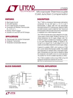
Transcription of LTC6362 - Precision, Low Power Rail-to-Rail Input/Output ...
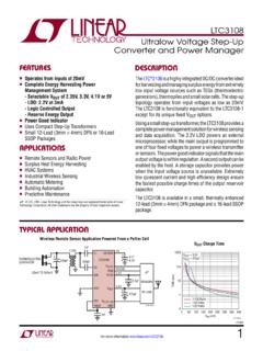
1 LTC636216362faTYPICAL APPLICATION FEATURESDESCRIPTIONP recision, Low Power Rail-to-Rail Input/Output Differential Op Amp/SAR ADC DriverThe LTC 6362 is a low Power , low noise differential op amp with Rail-to-Rail input and output swing that has been optimized to drive low Power SAR ADCs. The LTC6362 draws only 1mA of supply current in active operation, and features a shutdown mode in which the current consump-tion is reduced to 70 amplifier may be configured to convert a single-ended input signal to a differential output signal, and is capable of being operated in an inverting or noninverting configuration. Low offset voltage, low input bias current, and a stable high impedance configuration make this amplifier suit-able for use not only as an ADC driver but also earlier in the signal chain, to convert a precision sensor signal to a balanced (differential)
2 Signal for processing in noisy industrial LTC6362 is available in an 8-lead msop package and also in a compact 3mm 3mm 8-pin leadless DFN pack-age, and operates with guaranteed specifications over a 40 C to 125 C temperature Interface from a Ground-Referenced Single-Ended Input to an LTC2379-18 SAR ADCAPPLICATIONSn 1mA Supply Currentn Single to supplyn Fully Differential Input and Outputn 200 V Max Offset Voltagen 260nA Max Input Bias Currentn Fast Settling: 550ns to 18-Bit, 8VP-P Outputn Low Distortion: 116dBc at 1kHz, 8VP-Pn Rail-to-Rail Inputs and Outputsn Hz Input-Referred Noisen 180 MHz Gain-Bandwidth Productn 34 MHz 3dB Bandwidthn Low Power Shutdown: 70 An 8-Lead msop and 3mm 3mm 8-Lead DFN Packagesn 16-Bit and 18-Bit SAR ADC Driversn Single-Ended-to-Differential Conversionn Low Power Pipeline ADC Drivern Differential Line Driversn Battery-Powered InstrumentationL, LT, LTC, LTM, Linear Technology and the Linear logo are registered trademarks of Linear Technology Corporation.
3 All other trademarks are the property of their respective owners. ++ +VREFVDD5 VLTC2379-18 SAR FVIN1k1k1k1kSHDNLTC6362 Driving LTC2379-18 fIN = 2kHz, 1dBFS, 16384-Point FFTFREQUENCY (kHz)0 150 140 AMPLITUDE (dBFS) 120 100 800 40100200500 600 700 20 60 130 110 90 10 50 30 703004008006362 TA01bVS = 5V, 0 VVOUTDIFF = = = = = = = MAXIMUM RATINGSPIN CONFIGURATIONT otal Supply Voltage (V+ V ) .. Current (+IN, IN, VOCM, SHDN) (Note 2) .. 10 m AOutput Short-Circuit Duration (Note 3) ..IndefiniteOperating Temperature Range (Note 4) LTC6 362C/ LTC6 362I .. 40 C to 85 C LTC6 362H .. 40 C to 125 C(Note 1)1234 INVOCMV++OUT8765+INSHDNV OUTTOP VIEWMS8 PACKAGE8-LEAD PLASTIC msop TJMAX = 150 C, JA = 273 C/W, JC = 45 C/WTOP VIEW9V DD PACKAGE8-LEAD (3mm 3mm) PLASTIC DFN56784321 INVOCMV++OUT+INSHDNV OUTTJMAX = 150 C, JA = C/W, JC = 45 C/WEXPOSED PAD (PIN 9) IS V , MUST BE SOLDERED TO PCBORDER INFORMATIONLEAD FREE FINISHTAPE AND REELPART MARKING*PACKAGE DESCRIPTIONSPECIFIED TEMPERATURE RANGELTC6362 CMS8#PBFLTC6362 CMS8#TRPBFLTGCN8-Lead Plastic MSOP0 C to 70 CLTC6362 IMS8#PBFLTC6362 IMS8#TRPBFLTGCN8-Lead Plastic msop 40 C to 85 CLTC6362 HMS8#PBFLTC6362 HMS8#TRPBFLTGCN8-Lead Plastic msop 40 C to 125 CLTC6362 CDD#PBFLTC6362 CDD#TRPBFLGCM8-Lead (3mm 3mm)
4 Plastic DFN0 C to 70 CLTC6362 IDD#PBFLTC6362 IDD#TRPBFLGCM8-Lead (3mm 3mm) Plastic DFN 40 C to 85 CLTC6362 HDD#PBFLTC6362 HDD#TRPBFLGCM8-Lead (3mm 3mm) Plastic DFN 40 C to 125 CConsult LTC Marketing for parts specified with wider operating temperature ranges. *The temperature grade is identified by a label on the shipping container. Consult LTC Marketing for information on non-standard lead based finish more information on lead free part marking, go to: For more information on tape and reel specifications, go to: Temperature Range (Note 5) LTC6 362C ..0 C to 70 C LTC6 362I .. 40 C to 85 C LTC6 362H .. 40 C to 125 CMaximum Junction Temperature ..150 CStorage Temperature Range .. 65 C to 150 CLTC636236362faELECTRICAL CHARACTERISTICS The l denotes the specifications which apply over the full operating temperature range, otherwise specifications are at TA = 25 C.
5 V+ = 5V, V = 0V, VCM = VOCM = VICM = , VSHDN = open. VS is defined as (V+ V ). VOUTCM is defined as (V+OUT + V OUT)/2. VICM is defined as (V+IN + V IN)/2. VOUTDIFF is defined as (V+OUT V OUT).SYMBOLPARAMETERCONDITIONSMINTYPMAXU NITSVOSDIFF (Note 6)Differential Offset Voltage (Input Referred)VS = 3V VICM = VICM = l l 50 65 200 350 250 600 V V V VVS = 5V VICM = VICM = l l 50 75 200 350 260 600 V V V V VOSDIFF/ T (Note 7)Differential Offset Voltage Drift (Input Referred)VS = 3V VS = 5V l V/ C V/ CIB (Note 8)Input Bias CurrentVS = 3V VICM = VICM = l l 100 75 350 500 350 850 nA nA nA nAVS = 5V VICM = VICM = l l 75 75 260 460 350 850 nA nA nA nA IB/ TInput Bias Current DriftVS = 3V VS = 5Vl C nA/ CIOS (Note 8)
6 Input Offset CurrentVS = 3V VICM = VICM = l l 75 125 325 650 425 1200 nA nA nA nAVS = 5V VICM = VICM = l l 75 125 325 500 425 1200 nA nA nA nARINI nput ResistanceCommon Mode Differential Mode14 32M k CINI nput CapacitanceDifferential Mode 2pFenDifferential Input Noise Voltage Densityf = 100kHz, Not Including RI/RF Hz inInput Noise Current Densityf = 100kHz, Not Including RI/RF HzenvocmCommon Mode Noise Voltage Densityf = HzVICMR (Note 9)Input Common Mode RangeVS = 3V VS = 5Vl l0 03 5V VCMRRI (Note 10)Input Common Mode Rejection Ratio (Input Referred) VICM/ VOSDIFFVS = 3V, VICM from 0V to 3V VS = 5V, VICM from 0V to 5Vl l70 7395 98dB dBCMRRIO (Note 10)Output Common Mode Rejection Ratio (Input Referred) VOCM/ VOSDIFFVS = 3V, VOCM from to VS = 5V, VOCM from to l75 55100 90dB dBPSRR (Note 11)Differential Power Supply Rejection ( VS/ VOSDIFF)VS = to (Note 11)Output Common Mode Power Supply Rejection ( VS/ VOSCM)VS = to dBLTC636246362faELECTRICAL CHARACTERISTICS The l denotes the specifications which apply over the full operating temperature range, otherwise specifications are at TA = 25 C.
7 V+ = 5V, V = 0V, VCM = VOCM = VICM = , VSHDN = open. VS is defined as (V+ V ). VOUTCM is defined as (V+OUT + V OUT)/2. VICM is defined as (V+IN + V IN)/2. VOUTDIFF is defined as (V+OUT V OUT).SYMBOLPARAMETERCONDITIONSMINTYPMAXU NITSGCMC ommon Mode Gain ( VOUTCM/ VOCM) VS = 3V, VOCM from to VS = 5V, VOCM from to l1 1V/V V/V GCMC ommon Mode Gain Error 100 (GCM 1)VS = 3V, VOCM from to VS = 5V, VOCM from to l %BALO utput Balance ( VOUTCM/ VOUTDIFF) VOUTDIFF = 2V Single-Ended Input Differential Input l l 57 57 35 35 dB dBAVOLOpen-Loop Voltage Gain95dBVOSCMC ommon Mode Offset Voltage (VOUTCM VOCM)VS = 3V VS = 5Vl l 6 6 30 30mV mV VOSCM/ TCommon Mode Offset Voltage Driftl45 V/ CVOUTCMR (Note 9)Output Signal Common Mode Range (Voltage Range for the VOCM Pin)
8 VOCM Driven Externally, VS = 3V VOCM Driven Externally, VS = 5Vl VVOCMSelf-Biased Voltage at the VOCM PinVOCM Not Connected, VS = 3V VOCM Not Connected, VS = 5Vl VRINVOCMI nput Resistance, VOCM Pinl110170230k VOUT Output Voltage, High, Either Output PinIL= 0mA, VS = 3V IL = 5mA, VS = 3Vl VIL= 0mA, VS = 5V IL = 5mA, VS = 5Vl VOutput Voltage, Low , Either Output PinIL= 0mA, VS = 3V IL = 5mA, VS = 3Vl VIL= 0mA, VS = 5V IL = 5mA, VS = 5Vl VISCO utput Short-Circuit Current, Either Output PinVS = 3V VS = 5Vl l13 1525 35mA mASRSlew Rate Differential 8VP-P Output45V/ sGBWPGain-Bandwidth ProductfTEST = 200kHz l145 90180 MHz MHzf 3dB 3dB BandwidthRI = RF = 1k34 MHzHD2/HD32nd/3rd Order Harmonic Distortion Single-Ended Inputf = 1kHz, VOUT = 8VP-P f = 10kHz, VOUT = 8VP-P f = 100kHz, VOUT = 8VP-P 120/ 116 106/ 103 84/ 76dBc dBc dBctsSettling Time to a 2VP-P Output (16-Bit) 4ppm (18-Bit)160 180 230 440ns ns ns nsSettling Time to a 8VP-P Output (16-Bit) 4ppm (18-Bit)230 300 460 550ns ns ns nsVS (Note 12)
9 Supply Voltage CurrentVS = 3V, Active mAVS = 3V, Shutdownl55130 AVS = 5V, Active mAVS = 5V, Shutdownl70140 ALTC636256362faELECTRICAL CHARACTERISTICS The l denotes the specifications which apply over the full operating temperature range, otherwise specifications are at TA = 25 C. V+ = 5V, V = 0V, VCM = VOCM = VICM = , VSHDN = open. VS is defined as (V+ V ). VOUTCM is defined as (V+OUT + V OUT)/2. VICM is defined as (V+IN + V IN)/2. VOUTDIFF is defined as (V+OUT V OUT).Note 1: Stresses beyond those listed under Absolute Maximum Ratings may cause permanent damage to the device.
10 Exposure to any Absolute Maximum Rating condition for extended periods may affect device reliability and 2: Input pins (+IN, IN, VOCM and SHDN) are protected by steering diodes to either supply. If the inputs should exceed either supply voltage, the input current should be limited to less than 10mA. In addition, the inputs +IN, IN are protected by a pair of back-to-back diodes. If the differential input voltage exceeds , the input current should be limited to less than 3: A heat sink may be required to keep the junction temperature below the absolute maximum rating when the output is shorted 4: The LTC6362C and LTC6362I are guaranteed functional over the operating temperature range of 40 C to 85 C. The LTC6362H is guaranteed functional over the operating temperature range of 40 C to 125 5: The LTC6362C is guaranteed to meet specified performance from 0 C to 70 LTC6362I is guaranteed to meet specified performance from 40 C to 85 C.
