Transcription of LTC6992-1/LTC6992-2/ LTC6992-3/LTC6992-4 - …
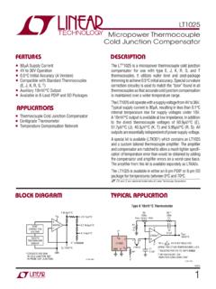
1 LTC6992-1/LTC6992-2/. LTC6992-3/LTC6992-4 . TimerBlox: Voltage-Controlled Pulse Width Modulator (PWM). Features Description n Pulse Width Modulation (PWM) Controlled by The LTC 6992 is a silicon oscillator with an easy-to-use Simple 0V to 1V Analog Input analog voltage-controlled pulse width modulation (PWM). n Four Available Options Define Duty Cycle Limits capability. The LTC6992 is part of the TimerBlox family Minimum Duty Cycle at 0% or 5% of versatile silicon timing devices. Maximum Duty Cycle at 95% or 100% A single resistor, RSET, programs the LTC6992's inter- n Frequency Range: to 1 MHz nal master oscillator frequency. The output frequency n Configured with 1 to 3 Resistors is determined by this master oscillator and an internal n < Maximum Frequency Error frequency divider, NDIV, programmable to eight settings n PWM Duty Cycle Error < Maximum from 1 to 16384. n Frequency Modulation (VCO) Capability n to Single Supply Operation 1 MHz 50k.
2 FOUT = , N = 1,4,16 16384. n 115 A Supply Current at 100kHz NDIV RSET DIV. n 500 s Start-Up Time n CMOS Output Driver Sources/Sinks 20mA. Applying a voltage between 0V and 1V on the MOD pin n 55 C to 125 C Operating Temperature Range sets the duty cycle. n Available in Low Profile (1mm) SOT-23 (ThinSOT ) The four versions differ in their minimum/maximum duty and 2mm 3mm DFN cycle. Note that a minimum duty cycle limit of 0% or maximum duty cycle limit of 100% allows oscillations to stop at the extreme duty cycle settings. Applications DEVICE NAME PWM DUTY CYCLE RANGE. n PWM Servo Loops LTC6992-1 0% to 100%. n Heater Control LTC6992-2 5% to 95%. n LED Dimming Control LTC6992-3 0% to 95%. n High Vibration, High Acceleration Environments LTC6992-4 5% to 100%. n Portable and Battery-Powered Equipment L, LT, LTC and LTM, Linear Technology, TimerBlox and the Linear logo are registered For easy configuration of the LTC6992, download the trademarks and ThinSOT is a trademark of Linear Technology Corporation.
3 All other trademarks TimerBlox Designer tool at are the property of their respective owners. Typical Application 1 MHz Pulse Width Modulator ANALOG PWM. DUTY CYCLE MOD OUT MOD. CONTROL (0V TO 1V) LTC6992 GND V+. C1. OUT. F. 1V/DIV. SET DIV. 6992 TA01a RSET. 50k 2 s/DIV 6992 TA01b 69921234fc 1. LTC6992-1/LTC6992-2/. LTC6992-3/LTC6992-4 . Absolute Maximum Ratings (Note 1). Supply Voltage (V+) to .6V Specified Temperature Range (Note 3). Maximum Voltage On Any Pin 0 C to 70 C..(GND ) VPIN (V+ + ) 40 C to 85 C. Operating Temperature Range (Note 2) 40 C to 125 C. 40 C to 85 C 55 C to 125 C. 40 C to 85 C Junction Temperature .. 150 C. 40 C to 125 C Storage Temperature 65 C to 150 C. 55 C to 125 C Lead Temperature (Soldering, 10 sec). S6 300 C. Pin Configuration TOP VIEW. TOP VIEW. V+ 1 6 OUT. MOD 1 6 OUT. 7. DIV 2 5 GND. GND GND 2 5 V+. SET 3 4 MOD SET 3 4 DIV. S6 PACKAGE. DCB PACKAGE. 6-LEAD PLASTIC TSOT-23.
4 6-LEAD (2mm 3mm) PLASTIC DFN. TJMAX = 150 C, JA = 192 C/W, JC = 51 C/W. TJMAX = 150 C, JA = 64 C/W, JC = C/W. EXPOSED PAD (PIN 7) IS GND, PCB CONNECTION IS OPTIONAL. Order Information Lead Free Finish TAPE AND REEL (MINI) TAPE AND REEL PART MARKING* PACKAGE DESCRIPTION SPECIFIED TEMPERATURE RANGE. LTC6992 CDCB-1#TRMPBF LTC6992 CDCB-1#TRPBF LDXC 6-Lead (2mm 3mm) Plastic DFN 0 C to 70 C. LTC6992 IDCB-1#TRMPBF LTC6992 IDCB-1#TRPBF LDXC 6-Lead (2mm 3mm) Plastic DFN 40 C to 85 C. LTC6992 HDCB-1#TRMPBF LTC6992 HDCB-1#TRPBF LDXC 6-Lead (2mm 3mm) Plastic DFN 40 C to 125 C. LTC6992CS6-1#TRMPBF LTC6992CS6-1#TRPBF LTDXB 6-Lead Plastic TSOT-23 0 C to 70 C. LTC6992IS6-1#TRMPBF LTC6992IS6-1#TRPBF LTDXB 6-Lead Plastic TSOT-23 40 C to 85 C. LTC6992HS6-1#TRMPBF LTC6992HS6-1#TRPBF LTDXB 6-Lead Plastic TSOT-23 40 C to 125 C. LTC6992 CDCB-2#TRMPBF LTC6992 CDCB-2#TRPBF LDXF 6-Lead (2mm 3mm) Plastic DFN 0 C to 70 C.
5 LTC6992 IDCB-2#TRMPBF LTC6992 IDCB-2#TRPBF LDXF 6-Lead (2mm 3mm) Plastic DFN 40 C to 85 C. LTC6992 HDCB-2#TRMPBF LTC6992 HDCB-2#TRPBF LDXF 6-Lead (2mm 3mm) Plastic DFN 40 C to 125 C. LTC6992CS6-2#TRMPBF LTC6992CS6-2#TRPBF LTDXD 6-Lead Plastic TSOT-23 0 C to 70 C. LTC6992IS6-2#TRMPBF LTC6992IS6-2#TRPBF LTDXD 6-Lead Plastic TSOT-23 40 C to 85 C. LTC6992HS6-2#TRMPBF LTC6992HS6-2#TRPBF LTDXD 6-Lead Plastic TSOT-23 40 C to 125 C. LTC6992 CDCB-3#TRMPBF LTC6992 CDCB-3#TRPBF LFCP 6-Lead (2mm 3mm) Plastic DFN 0 C to 70 C. LTC6992 IDCB-3#TRMPBF LTC6992 IDCB-3#TRPBF LFCP 6-Lead (2mm 3mm) Plastic DFN 40 C to 85 C. LTC6992 HDCB-3#TRMPBF LTC6992 HDCB-3#TRPBF LFCP 6-Lead (2mm 3mm) Plastic DFN 40 C to 125 C. LTC6992CS6-3#TRMPBF LTC6992CS6-3#TRPBF LTFCQ 6-Lead Plastic TSOT-23 0 C to 70 C. LTC6992IS6-3#TRMPBF LTC6992IS6-3#TRPBF LTFCQ 6-Lead Plastic TSOT-23 40 C to 85 C. LTC6992HS6-3#TRMPBF LTC6992HS6-3#TRPBF LTFCQ 6-Lead Plastic TSOT-23 40 C to 125 C.
6 69921234fc 2. LTC6992-1/LTC6992-2/. LTC6992-3/LTC6992-4 . ORDER INFORMATION. Lead Free Finish TAPE AND REEL (MINI) TAPE AND REEL PART MARKING* PACKAGE DESCRIPTION SPECIFIED TEMPERATURE RANGE. LTC6992 CDCB-4#TRMPBF LTC6992 CDCB-4#TRPBF LFCR 6-Lead (2mm 3mm) Plastic DFN 0 C to 70 C. LTC6992 IDCB-4#TRMPBF LTC6992 IDCB-4#TRPBF LFCR 6-Lead (2mm 3mm) Plastic DFN 40 C to 85 C. LTC6992 HDCB-4#TRMPBF LTC6992 HDCB-4#TRPBF LFCR 6-Lead (2mm 3mm) Plastic DFN 40 C to 125 C. LTC6992CS6-4#TRMPBF LTC6992CS6-4#TRPBF LTFCS 6-Lead Plastic TSOT-23 0 C to 70 C. LTC6992IS6-4#TRMPBF LTC6992IS6-4#TRPBF LTFCS 6-Lead Plastic TSOT-23 40 C to 85 C. LTC6992HS6-4#TRMPBF LTC6992HS6-4#TRPBF LTFCS 6-Lead Plastic TSOT-23 40 C to 125 C. LTC6992 MPS6-1#TRMPBF LTC6992 MPS6-1#TRPBF LTDXB 6-Lead Plastic TSOT-23 55 C to 125 C. LTC6992 MPS6-2#TRMPBF LTC6992 MPS6-2#TRPBF LTDXD 6-Lead Plastic TSOT-23 55 C to 125 C. LTC6992 MPS6-3#TRMPBF LTC6992 MPS6-3#TRPBF LTFCQ 6-Lead Plastic TSOT-23 55 C to 125 C.
7 LTC6992 MPS6-4#TRMPBF LTC6992 MPS6-4#TRPBF LTFCS 6-Lead Plastic TSOT-23 55 C to 125 C. TRM = 500 pieces. *Temperature grades are identified by a label on the shipping container. Consult LTC Marketing for parts specified with wider operating temperature ranges. Consult LTC Marketing for information on lead based finish parts. For more information on lead free part marking, go to: For more information on tape and reel specifications, go to: Electrical Characteristics The l denotes the specifications which apply over the full operating temperature range, otherwise specifications are at TA = 25 C. Test conditions are V+ = to , VMOD = 0V to VSET, DIVCODE = 0 to 15 (NDIV = 1 to 16,384), RSET = 50k to 800k, RLOAD = 5k, CLOAD = 5pF unless otherwise noted. SYMBOL PARAMETER CONDITIONS MIN TYP MAX UNITS. Oscillation Frequency fOUT Output Frequency 1000000 Hz fOUT Frequency Accuracy (Note 4) fOUT 1 MHz %. l %.
8 FOUT/ T Frequency Drift Over Temperature l %/ C. fOUT/ V+ Frequency Drift Over Supply V+ = to l %/V. V+ = to l %/V. Long-Term Frequency Stability (Note 10) 90 ppm/ kHr Period Jitter (Note 9) NDIV = 1 %P-P. NDIV = 4 %P-P. %RMS. NDIV = 16 %P-P. %RMS. Pulse Width Modulation D PWM Duty Cycle Accuracy VMOD = VSET to VSET %. VMOD = VSET to VSET l %. VMOD < VSET or VMOD > VSET l %. DMAX Maximum Duty Cycle Limit LTC6992-1/LTC6992-4, POL = 0, VMOD = 1V l 100 %. LTC6992-2/LTC6992-3, POL = 0, VMOD = 1V l 95 99 %. DMIN Minimum Duty Cycle Limit LTC6992-1/LTC6992-3, POL = 0, VMOD = 0V l 0 %. LTC6992-2/LTC6992-4, POL = 0, VMOD = 0V l 1 5 %. tS,PWM Duty Cycle Settling Time (Note 6) tMASTER = tOUT/NDIV 8 tMASTER s 69921234fc 3. LTC6992-1/LTC6992-2/. LTC6992-3/LTC6992-4 . Electrical Characteristics The l denotes the specifications which apply over the full operating temperature range, otherwise specifications are at TA = 25 C.
9 Test conditions are V+ = to , VMOD = 0V to VSET, DIVCODE = 0 to 15 (NDIV = 1 to 16,384), RSET = 50k to 800k, RLOAD = 5k, CLOAD = 5pF unless otherwise noted. SYMBOL PARAMETER CONDITIONS MIN TYP MAX UNITS. Power Supply V+ Operating Supply Voltage Range l V. Power-On Reset Voltage l V. IS Supply Current RL = , RSET = 50k, V+ = l 365 450 A. NDIV = 1 V+ = l 225 285 A. RL = , RSET = 50k, V+ = l 350 420 A. NDIV = 4 V+ = l 225 280 A. RL = , RSET = 50k, V+ = l 325 390 A. NDIV 16 V+ = l 215 265 A. RL = , RSET = 800k, V+ = l 120 170 A. NDIV = 1 to 16,384 V+ = l 105 150 A. Analog Inputs VSET Voltage at SET Pin l V. VSET/ T VSET Drift Over Temperature l 75 V/ C. RSET Frequency-Setting Resistor l 50 800 k . MOD Pin Input Capacitance pF. MOD Pin Input Current l 10 nA. VMOD,HI VMOD Voltage for Maximum LTC6992-1/LTC6992-4, POL = 0, D = 100% l VSET VSET V. Duty Cycle LTC6992-2/LTC6992-3, POL = 0, D = 95% VSET V.
10 VMOD,LO VMOD Voltage for Minimum LTC6992-1/LTC6992-3, POL = 0, D = 0% l VSET VSET V. Duty Cycle LTC6992-2/LTC6992-4, POL = 0, D = 5% VSET V. VDIV DIV Pin Voltage l 0 V+ V. VDIV/ V+ DIV Pin Valid Code Range (Note 5) Deviation from Ideal l %. VDIV/V+ = (DIVCODE + )/16. DIV Pin Input Current l 10nA. Digital Output IOUT(MAX) Output Current V+ = to 20 mA. VOH High Level Output Voltage (Note 7) V+ = IOUT = 1mA l V. IOUT = 16mA l V. V+ = IOUT = 1mA l V. IOUT = 10mA l V. V+ = IOUT = 1mA l V. IOUT = -8mA l V. VOL Low Level Output Voltage (Note 7) V+ = IOUT = 1mA l V. IOUT = 16mA l V. V+ = IOUT = 1mA l V. IOUT = 10mA l V. V+ = IOUT = 1mA l V. IOUT = 8mA l V. tr Output Rise Time (Note 8) V+ = , RLOAD = ns V+ = , RLOAD = ns V+ = , RLOAD = ns tf Output Fall Time (Note 8) V+ = , RLOAD = ns V+ = , RLOAD = ns V+ = , RLOAD = ns 69921234fc 4. LTC6992-1/LTC6992-2/. LTC6992-3/LTC6992-4 . Electrical Characteristics Note 1: Stresses beyond those listed under Absolute Maximum Ratings Note 7: To conform to the Logic IC Standard, current out of a pin is may cause permanent damage to the device.
