Transcription of LTC6993-1/LTC6993-2/LTC6993-3/LTC6993-4 - …
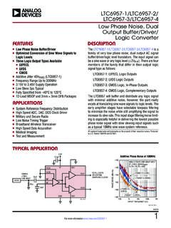
1 LTC6993-1/LTC6993-2 LTC6993-3/LTC6993-4169931234fcFor more information applicaTion FeaTuresDescripTionTimerBlox: Monostable Pulse Generator (One Shot)The LT C 6993 is a monostable multivibrator (also known as a one-shot pulse generator) with a programmable pulse width of 1 s to seconds. The LTC6993 is part of the TimerBlox family of versatile silicon timing single resistor, RSET, programs an internal master os-cillator frequency, setting the LTC6993 s time base. The output pulse width is determined by this master oscillator and an internal clock divider, NDIV , programmable to eight settings from 1 to 221. tOUT=NDIV RSET50k 1 s, NDIV = 1, 8, 64,..,221 The output pulse is initiated by a transition on the trigger input (TRIG).
2 Each part can be configured to generate posi-tive or negative output pulses. The LTC6993 is available in four versions to provide different trigger signal polarity and retrigger POLARITYRETRIGGERLTC6993-1 Rising-EdgeNoLTC6993-2 Rising-EdgeYesLTC6993-3 Falling-EdgeNoLTC6993-4 Falling-EdgeYesThe LTC6993 also offers the ability to dynamically adjust the width of the output pulse via a separate control easy configuration of the LTC6993, download the TimerBlox Designer tool at DetectorapplicaTions nPulse Width Range: 1 s to Seconds nConfigured with 1 to 3 Resistors nPulse Width Max Error: n< for Pulse Width > 512 s n< for Pulse Width of 8 s to 512 s n< for Pulse Width of 1 s to 8 s nFour LTC6993 Options Available.
3 NRising-Edge or Falling-Edge Trigger nRetriggerable or Non-Retriggerable nConfigurable for Positive or Negative Output Pulse nFast Recovery Time to Single Supply Operation n70 A Supply Current at 10 s Pulse Width n500 s Start-Up Time nCMOS Output Driver Sources/Sinks 20mA n 55 C to 125 C Operating Temperature Range nAvailable in Low Profile (1mm) SOT-23 (ThinSOT )and 2mm 3mm DFN nWatchdog Timer nFrequency Discriminators nMissing Pulse Detection nEnvelope Detection nHigh Vibration, High Acceleration Environments nPortable and Battery-Powered EquipmentL, LT, LTC, LTM, Linear Technology, TimerBlox and the Linear logo are registered trademarks and ThinSOT is a trademark of Linear Technology Corporation.
4 All other trademarks are the property of their respective TA01aLTC6993-2 OUTV+ FSIGNALENVELOPEMODULATEDCARRIERTRIG2V/DI VOUT2V/DIV50 s/DIV69931234 TA01b80kHz CARRIER16 sLTC6993-1/LTC6993-2 LTC6993-3/LTC6993-4269931234fcFor more information MaxiMuM raTingsSupply Voltage (V+) to GND ..6 VMaximum Voltage on Any (GND ) VPIN (V+ + )Operating Temperature Range (Note 2) LTC6993C .. 40 C to 85 C LTC6993I .. 40 C to 85 C LTC6993H .. 40 C to 125 C LTC6993MP .. 55 C to 125 C(Note 1)orDer inForMaTionTAPE AND REEL (MINI)TAPE AND REELPART MARKING*PACKAGE DESCRIPTIONSPECIFIED TEMPERATURE RANGELTC6993 CDCB-1#TRMPBF LTC6993 CDCB-1#TRPBFLDXH6-Lead (2mm 3mm) Plastic DFN0 C to 70 CLTC6993 IDCB-1#TRMPBFLTC6993 IDCB-1#TRPBFLDXH6-Lead (2mm 3mm) Plastic DFN 40 C to 85 CLTC6993 HDCB-1#TRMPBF LTC6993 HDCB-1#TRPBFLDXH6-Lead (2mm 3mm) Plastic DFN 40 C to 125 CLTC6993 CDCB-2#TRMPBF LTC6993 CDCB-2#TRPBFLDXK6-Lead (2mm 3mm) Plastic DFN0 C to 70 CLTC6993 IDCB-2#TRMPBFLTC6993 IDCB-2#TRPBFLDXK6-Lead (2mm 3mm) Plastic DFN 40 C to 85 CLTC6993 HDCB-2#TRMPBF LTC6993 HDCB-2#TRPBFLDXK6-Lead (2mm 3mm)
5 Plastic DFN 40 C to 125 CLTC6993 CDCB-3#TRMPBF LTC6993 CDCB-3#TRPBFLFMJ6-Lead (2mm 3mm) Plastic DFN0 C to 70 CLTC6993 IDCB-3#TRMPBFLTC6993 IDCB-3#TRPBFLFMJ6-Lead (2mm 3mm) Plastic DFN 40 C to 85 CLTC6993 HDCB-3#TRMPBF LTC6993 HDCB-3#TRPBFLFMJ6-Lead (2mm 3mm) Plastic DFN 40 C to 125 CLTC6993 CDCB-4#TRMPBF LTC6993 CDCB-4#TRPBFLFMM6-Lead (2mm 3mm) Plastic DFN0 C to 70 CLTC6993 IDCB-4#TRMPBFLTC6993 IDCB-4#TRPBFLFMM6-Lead (2mm 3mm) Plastic DFN 40 C to 85 CLTC6993 HDCB-4#TRMPBF LTC6993 HDCB-4#TRPBFLFMM6-Lead (2mm 3mm) Plastic DFN 40 C to 125 CLTC6993CS6-1#TRMPBFLTC6993CS6-1#TRPBFLT DXG6-Lead Plastic TSOT-230 C to 70 CLTC6993IS6-1#TRMPBFLTC6993IS6-1#TRPBFLT DXG6-Lead Plastic TSOT-23 40 C to 85 CLTC6993HS6-1#TRMPBFLTC6993HS6-1#TRPBFLT DXG6-Lead Plastic TSOT-23 40 C to 125 CTOP VIEWOUTGNDTRIGV+DIVSETDCB PACKAGE6-LEAD (2mm 3mm) PLASTIC DFN4576321 TJMAX = 150 C, JA = 64 C/W, JC = C/WEXPOSED PAD (PIN 7) CONNECTED TO GND, PCB CONNECTION OPTIONALTRIG 1 GND 2 SET 36 OUT5 V+4 DIVTOP VIEWS6 PACKAGE6-LEAD PLASTIC TSOT-23 TJMAX = 150 C, JA = 192 C/W, JC = 51 C/Wpin conFiguraTionSpecified Temperature Range (Note 3) LTC6993C.
6 0 C to 70 C LTC6993I .. 40 C to 85 C LTC6993H .. 40 C to 125 C LTC6993MP .. 55 C to 125 CJunction Temperature ..150 CStorage Temperature Range .. 65 C to 150 CLead Temperature (Soldering, 10 sec) S6 Package ..300 CLead Free FinishLTC6993-1/LTC6993-2 LTC6993-3/LTC6993-4369931234fcFor more information characTerisTics The l denotes the specifications which apply over the full operating temperature range, otherwise specifications are at TA = 25 C. Test conditions are V+ = to , TRIG = 0V, DIVCODE = 0 to 15 (NDIV = 1 to 221), RSET = 50k to 800k, RLOAD = 5k, CLOAD = 5pF unless otherwise AND REEL (MINI)
7 TAPE AND REELPART MARKING*PACKAGE DESCRIPTIONSPECIFIED TEMPERATURE RANGELTC6993CS6-2#TRMPBFLTC6993CS6-2#TRP BFLTDXJ6-Lead Plastic TSOT-230 C to 70 CLTC6993IS6-2#TRMPBFLTC6993IS6-2#TRPBFLT DXJ6-Lead Plastic TSOT-23 40 C to 85 CLTC6993HS6-2#TRMPBFLTC6993HS6-2#TRPBFLT DXJ6-Lead Plastic TSOT-23 40 C to 125 CLTC6993CS6-3#TRMPBFLTC6993CS6-3#TRPBFLT FMH6-Lead Plastic TSOT-230 C to 70 CLTC6993IS6-3#TRMPBFLTC6993IS6-3#TRPBFLT FMH6-Lead Plastic TSOT-23 40 C to 85 CLTC6993HS6-3#TRMPBFLTC6993HS6-3#TRPBFLT FMH6-Lead Plastic TSOT-23 40 C to 125 CLTC6993CS6-4#TRMPBFLTC6993CS6-4#TRPBFLT FMK6-Lead Plastic TSOT-230 C to 70 CLTC6993IS6-4#TRMPBFLTC6993IS6-4#TRPBFLT FMK6-Lead Plastic TSOT-23 40 C to 85 CLTC6993HS6-4#TRMPBFLTC6993HS6-4#TRPBFLT FMK6-Lead Plastic TSOT-23 40 C to 125 CLTC6993 MPS6-1#TRMPBF LTC6993 MPS6-1#TRPBFLTDXG6-Lead Plastic TSOT-23 55 C to 125 CLTC6993 MPS6-2#TRMPBF LTC6993 MPS6-2#TRPBFLTDXJ6-Lead Plastic TSOT-23 55 C to 125 CLTC6993 MPS6-3#TRMPBF LTC6993 MPS6-3#TRPBFLTFMH6-Lead Plastic TSOT-23 55 C to 125 CLTC6993 MPS6-4#TRMPBF LTC6993 MPS6-4#TRPBFLTFMK6-Lead Plastic TSOT-23 55 C to 125 CTRM = 500 pieces.
8 *Temperature grades are identified by a label on the shipping LTC Marketing for parts specified with wider operating temperature more information on lead free part marking, go to: For more information on tape and reel specifications, go to: Some packages are available in 500 unit reels through designated sales channels with #TRMPBF inForMaTionSYMBOLPARAMETERCONDITIONSMINT YPMAXUNITStOUTO utput Pulse Width1 tOUTP ulse Width Accuracy (Note 4)NDIV 512 l %8 NDIV 64 l %NDIV = 1 (LTC6993-1 or LTC6993-2) l %NDIV = 1 (LTC6993-3 or LTC6993-4) l % tOUT/ TPulse Width Drift Over TemperatureNDIV 512 NDIV 64l l C %/ CPulse Width Change With SupplyNDIV 512 V+ = to V+ = to l %8 NDIV 64 V+ = to V+ = to V+ = to l l % %Lead Free FinishLTC6993-1/LTC6993-2 LTC6993-3/LTC6993-4469931234fcFor more information characTerisTics The l denotes the specifications which apply over
9 The full operating temperature range, otherwise specifications are at TA = 25 C. Test conditions are V+ = to , TRIG = 0V, DIVCODE = 0 to 15 (NDIV = 1 to 221), RSET = 50k to 800k, RLOAD = 5k, CLOAD = 5pF unless otherwise Width Jitter (Note 10)NDIV = 1 V+ = V+ = %P-PNDIV = = = = Width Change Settling Time (Note 9) tMASTER = tOUT/NDIV6 tMASTER sPower SupplyV+Operating Supply Voltage Reset (IDLE)Supply Current (Idle)RL = , RSET = 50k, NDIV 64 V+ = V+ = l165 125200 160 A ARL = , RSET = 50k, NDIV 512 V+ = V+ = l135 105175 140 A ARL = , RSET = 800k, NDIV 64 V+ = V+ = l70 60110 95 A ARL = , RSET = 800k, NDIV 512 V+ = V+ = l65 55100 90 A AAnalog InputsVSETV oltage at SET VSET/ TVSET Drift Over Temperaturel 75 V/ CRSETF requency-Setting Resistorl50800k VDIVDIV Pin Voltagel0V+V VDIV/ V+DIV Pin Valid Code Range (Note 5)Deviation from Ideal VDIV/V+ = (DIVCODE + )
10 /16l Pin Input Currentl 10nADigital I/OTRIG Pin Input Pin Input CurrentTRIG = 0V to V+ 10nAVIHHigh Level TRIG Pin Input Voltage(Note 6) V+VVILLow Level TRIG Pin Input Voltage(Note 6) V+VIOUT(MAX)Output CurrentV+ = to 20mAVOHHigh Level Output Voltage (Note 7)V+ = IOUT = 1mA IOUT = 16mAl VV+ = IOUT = 1mA IOUT = 10mAl VV+ = IOUT = 1mA IOUT = 8mAl VVOLLow Level Output Voltage (Note 7)V+ = IOUT = 1mA IOUT = 16mAl VV+ = IOUT = 1mA IOUT = 10mAl VV+ = IOUT = 1mA IOUT = 8mAl VLTC6993-1/LTC6993-2 LTC6993-3/LTC6993-4569931234fcFor more information characTerisTicsNote 1: Stresses beyond those listed under Absolute Maximum Ratings may cause permanent damage to the device.